PCB Spiral Trace Routing: Advantages and Disadvantages Compared
Introduction
Printed Circuit Board (PCB) design involves numerous routing techniques, each with specific applications and implications for circuit performance. Among these techniques, spiral trace routing has gained attention for its unique properties in various electronic applications. This 2000-word article provides a comprehensive comparison of the advantages and disadvantages of using spiral traces in PCB design, examining their electrical characteristics, manufacturing considerations, and practical applications.
Understanding Spiral Traces in PCB Design
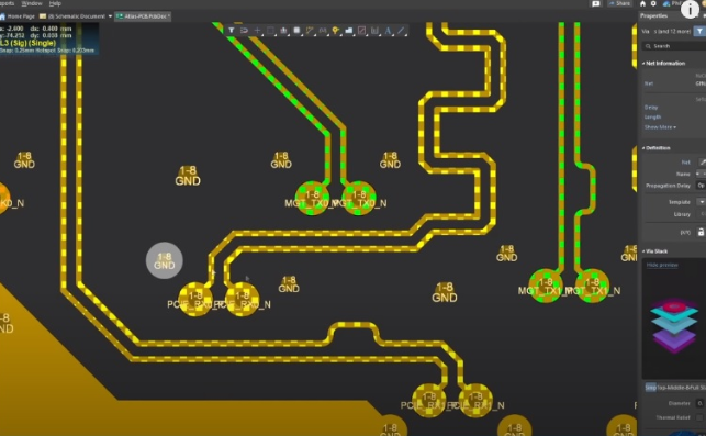
Spiral traces refer to conductive pathways on a PCB that follow a circular or rectangular spiral pattern, either as single turns or multiple concentric loops. These traces can be implemented in various configurations:
- Single-layer spirals: Confined to one PCB layer
- Multi-layer spirals: Spanning across multiple layers with vias
- Circular spirals: Smooth curved patterns
- Rectangular spirals: Angular turns for easier manufacturing
The specific geometry and implementation of spiral traces significantly influence their performance characteristics and suitability for different applications.
Advantages of PCB Spiral Traces
1. Compact Inductor Implementation
Space Efficiency: Spiral traces allow the creation of planar inductors directly on the PCB, saving significant board space compared to discrete inductor components. This is particularly valuable in miniaturized designs where every square millimeter counts.
Predictable Inductance: The inductance of a spiral trace can be calculated with reasonable accuracy using established formulas that account for:
- Number of turns
- Trace width
- Spacing between turns
- Outer diameter
- Inner diameter
This predictability enables designers to implement specific inductance values without additional components.
2. Improved Signal Integrity in Certain Applications
Controlled Impedance: When properly designed, spiral traces can maintain consistent impedance throughout their length, reducing reflections in high-speed signals.
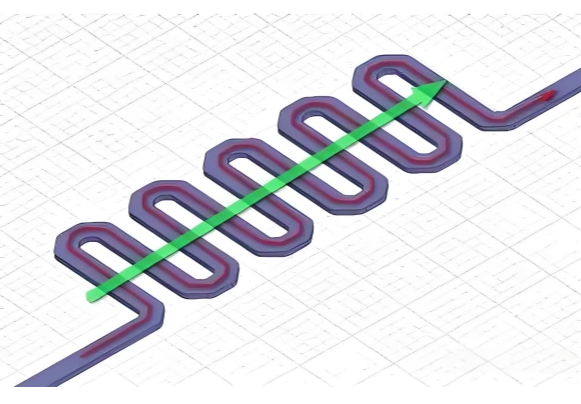
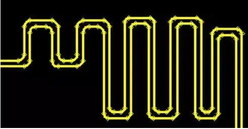
Delay Lines: The extended path length in a compact area makes spirals useful for implementing precise time delays in signal paths, particularly in clock distribution networks and timing circuits.
3. EMI Reduction Benefits
Controlled Magnetic Fields: The opposing current directions in adjacent turns of a spiral can help cancel out magnetic fields, reducing electromagnetic interference (EMI) in sensitive circuits.
Shielding Effects: Multi-layer spiral configurations can provide some degree of electromagnetic shielding for sensitive components when properly implemented.
4. Thermal Management Applications
Heat Distribution: The extended trace length and geometric pattern of spirals can help distribute heat more evenly across a PCB, particularly when used in power delivery networks.
Thermal Relief: Spiral patterns can be incorporated into thermal pads to control heat transfer during soldering processes.
5. RF and Microwave Circuit Advantages
Distributed Elements: At high frequencies, spiral traces can function as distributed elements (inductors, transformers, or resonators), eliminating the need for discrete components that might introduce parasitic effects.
Miniaturized RF Circuits: Spiral inductors are essential components in many RF integrated circuits and system-on-chip designs where space is at a premium.
Disadvantages of PCB Spiral Traces
1. Manufacturing Challenges
Precision Requirements: High-quality spiral traces, especially for RF applications, require tight manufacturing tolerances that may increase fabrication costs.
Yield Issues: Imperfections in spiral traces (such as variations in trace width or spacing) can significantly affect performance, potentially reducing manufacturing yields.
Layer-to-Layer Alignment: For multi-layer spirals, precise alignment between layers is critical, requiring advanced PCB manufacturing capabilities.
2. Electrical Performance Limitations
Quality Factor (Q): PCB spiral inductors typically have lower Q factors compared to discrete components due to:
- Substrate losses
- Limited conductor thickness
- Proximity effects between turns
Parasitic Capacitance: The close proximity of turns in a spiral creates parasitic capacitance that can limit high-frequency performance and create unwanted resonances.
Current Handling Capacity: The typically narrow traces used in spirals limit their current-carrying capacity compared to discrete inductors with thicker windings.
3. Design Complexity
Simulation Requirements: Accurate modeling of spiral traces requires advanced electromagnetic simulation tools, adding complexity to the design process.
Layout Challenges: Routing other traces near or through spiral structures requires careful consideration to avoid unwanted coupling or interference.
Tuning Difficulties: Once fabricated, the characteristics of spiral traces cannot be easily adjusted, unlike discrete components which can be swapped or tuned.
4. Frequency Limitations
Skin Effect: At higher frequencies, current crowds to the outer surface of conductors, increasing resistive losses in spiral traces.
Substrate Losses: Dielectric materials in standard PCBs can introduce significant losses at microwave frequencies, limiting the effectiveness of spiral structures.
Self-Resonance: The combination of inductance and parasitic capacitance creates a self-resonant frequency beyond which the spiral behaves as a capacitor rather than an inductor.
Comparative Analysis: Spiral Traces vs. Alternative Approaches
Spiral Traces vs. Discrete Inductors
| Characteristic | Spiral Traces | Discrete Inductors |
|---|---|---|
| Size | Compact | Larger |
| Cost | Lower (no additional component) | Higher |
| Q Factor | Lower (typically 10-30) | Higher (can exceed 100) |
| Current Handling | Limited by trace width | Higher (thicker windings) |
| Precision | Fixed after fabrication | Adjustable |
| Parasitics | Higher inter-winding capacitance | Lower (depending on type) |
Spiral Traces vs. Straight Trace Inductors
| Characteristic | Spiral Traces | Straight Traces |
|---|---|---|
| Inductance Density | Higher | Lower |
| Area Efficiency | Better | Worse |
| Mutual Coupling | Higher between turns | Lower |
| Proximity Effects | More significant | Less significant |
| Radiation | More contained | More directional |
Practical Applications and Case Studies
1. RF Matching Networks
Spiral traces are commonly used in impedance matching networks for RF circuits, particularly in:
- Antenna matching circuits
- Filter implementations
- Oscillator tank circuits
Example: A 2.4GHz WiFi front-end module might use spiral inductors for impedance matching between the power amplifier and antenna.
2. Power Electronics
In DC-DC converters, spiral inductors can be implemented directly on the PCB for:
- Low-current voltage regulators
- Point-of-load converters
- Energy harvesting circuits
Limitation: Typically limited to currents below 1-2A due to trace width constraints.
3. Sensor Applications
Spiral traces are used in:
- Proximity sensors
- Metal detectors
- Biomedical sensors (e.g., NMR coils)
Advantage: The planar nature allows close coupling to measured objects.

Design Considerations for Optimal Spiral Trace Implementation
- Trace Width Selection: Balance between resistance (wider better) and turn density (narrower allows more turns)
- Spacing Between Turns: Affects both mutual coupling and parasitic capacitance
- Number of Turns: More turns increase inductance but also resistance and parasitic capacitance
- Layer Utilization: Multi-layer spirals can improve performance but increase complexity
- Ground Plane Effects: Proper ground plane placement can reduce unwanted coupling
- Material Selection: High-frequency applications may require specialized low-loss substrates
Future Trends and Developments
- 3D Printed Electronics: Additive manufacturing may enable more complex spiral geometries
- Embedded Passives: Spiral inductors integrated into substrate layers
- Advanced Materials: Use of low-loss dielectric materials to improve Q factor
- AI-Optimized Designs: Machine learning algorithms for optimizing spiral geometries
- Hybrid Approaches: Combining PCB spirals with discrete components for balanced performance
Conclusion
PCB spiral trace routing offers a valuable tool for circuit designers, particularly in space-constrained and high-frequency applications. The advantages of compact size, integration capability, and cost-effectiveness make spirals attractive for many modern electronic designs. However, the limitations in quality factor, current handling, and high-frequency performance mean that spiral traces are not universally superior to alternative approaches.
The decision to use spiral traces should be based on a careful evaluation of the specific application requirements, considering factors such as frequency range, current levels, available board space, and performance tolerances. As PCB manufacturing technologies continue to advance, many of the current limitations of spiral traces may be mitigated, expanding their range of applications in electronic design.
For optimal results, designers should:
- Use electromagnetic simulation tools to verify spiral performance
- Consider prototyping critical spiral structures
- Evaluate trade-offs between spiral implementations and discrete components
- Stay informed about new materials and manufacturing techniques that may improve spiral trace performance
By understanding both the advantages and disadvantages of PCB spiral traces, engineers can make informed decisions about when and how to implement these structures in their designs, balancing performance requirements with practical manufacturing considerations.