PCB Sub-Assembly: A Comprehensive Guide to the Backbone of Modern Electronics
Introduction
Printed Circuit Boards (PCBs) are the foundation of modern electronics, providing the necessary electrical connections and mechanical support for electronic components. However, a PCB alone is not enough to create a functional electronic device. It requires the integration of various components, such as resistors, capacitors, integrated circuits (ICs), connectors, and more, to form a complete system. This process of assembling and integrating components onto a PCB is known as PCB sub-assembly. PCB sub-assembly is a critical step in the manufacturing of electronic devices, as it determines the functionality, reliability, and performance of the final product. This article provides a comprehensive overview of PCB sub-assembly, covering its types, processes, challenges, applications, and future trends.
1. Understanding PCB Sub-Assembly
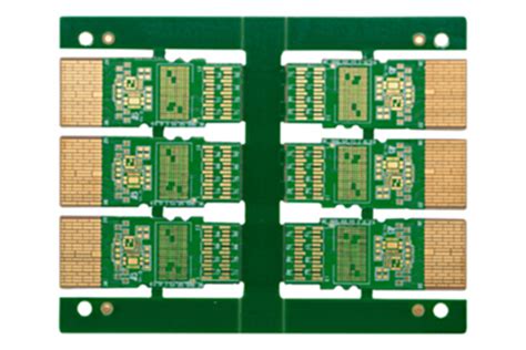
PCB sub-assembly refers to the process of mounting and soldering electronic components onto a PCB to create a functional circuit. The sub-assembly process transforms a bare PCB into a populated board that can perform specific electronic functions. Depending on the complexity of the design, a PCB sub-assembly may involve single-sided, double-sided, or multi-layer PCBs, as well as surface-mount technology (SMT) and through-hole technology (THT) components.
1.1 Types of PCB Sub-Assembly
- Single-Sided Sub-Assembly: Components are mounted and soldered on only one side of the PCB. This is typically used for simple, low-density designs.
- Double-Sided Sub-Assembly: Components are mounted and soldered on both sides of the PCB, allowing for higher component density and more complex circuits.
- Multi-Layer Sub-Assembly: Components are mounted on PCBs with multiple layers of conductive traces, enabling even greater complexity and functionality.
1.2 Key Components in PCB Sub-Assembly
- Resistors and Capacitors: Passive components that regulate current and store electrical energy.
- Integrated Circuits (ICs): Active components that perform complex functions, such as microprocessors and memory chips.
- Connectors: Components that provide electrical connections between the PCB and external devices.
- Diodes and Transistors: Semiconductor devices that control the flow of electrical current.
- Inductors and Transformers: Components that store energy in magnetic fields and transfer energy between circuits.
2. PCB Sub-Assembly Processes
The PCB sub-assembly process involves several steps, each requiring precision and attention to detail to ensure the quality and reliability of the final product.
2.1 Component Placement
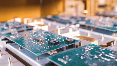
The first step in PCB sub-assembly is the placement of electronic components onto the PCB. This can be done manually for low-volume production or using automated pick-and-place machines for high-volume production. The components are placed according to the design specifications, ensuring accurate alignment and orientation.
2.2 Soldering
Soldering is the process of creating electrical and mechanical connections between the components and the PCB. There are two primary soldering techniques used in PCB sub-assembly:
- Surface-Mount Technology (SMT): SMT components are placed directly onto the surface of the PCB and soldered using reflow soldering. This technique is widely used for small, lightweight components and high-density designs.
- Through-Hole Technology (THT): THT components have leads that are inserted into holes drilled in the PCB and soldered on the opposite side. This technique is used for larger components and applications requiring strong mechanical bonds.
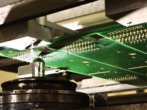
2.3 Inspection and Testing
After soldering, the assembled PCB undergoes inspection and testing to ensure it meets the required quality standards. Common inspection methods include:
- Visual Inspection: Manual or automated inspection to check for soldering defects, such as bridges, voids, or misaligned components.
- Automated Optical Inspection (AOI): A machine vision system that scans the PCB for defects and compares it to the design specifications.
- X-Ray Inspection: Used to inspect hidden solder joints, such as those in ball grid array (BGA) components.
- Functional Testing: Electrical testing to verify the functionality of the assembled PCB.
2.4 Cleaning
The assembled PCB is cleaned to remove flux residues, solder paste, and other contaminants that could affect performance or reliability. Cleaning methods include ultrasonic cleaning, vapor degreasing, and aqueous cleaning.
2.5 Conformal Coating
In some applications, the assembled PCB is coated with a protective layer (conformal coating) to protect it from moisture, dust, and other environmental factors. Common coating materials include acrylic, silicone, and urethane.
3. Challenges in PCB Sub-Assembly
PCB sub-assembly is a complex process that presents several challenges, including:
3.1 Miniaturization
The trend toward smaller, more compact electronic devices has led to the use of smaller components and higher-density designs. This increases the complexity of the sub-assembly process and requires advanced equipment and techniques.
3.2 Thermal Management
High-power components generate heat, which can affect the performance and reliability of the PCB. Effective thermal management, such as the use of heat sinks and thermal vias, is essential to dissipate heat and prevent overheating.
3.3 Component Compatibility
Ensuring compatibility between different components and materials is critical to avoid issues such as thermal expansion mismatch, chemical reactions, or electrical interference.
3.4 Quality Control
Maintaining consistent quality across large production runs is a significant challenge. Automated inspection and testing systems are essential to detect and address defects early in the process.
3.5 Cost and Lead Time
The cost and lead time of PCB sub-assembly can be significant, especially for complex designs or low-volume production. Balancing cost, quality, and speed is a key challenge for manufacturers.
4. Applications of PCB Sub-Assembly
PCB sub-assembly is used in a wide range of industries and applications, including:
4.1 Consumer Electronics
PCB sub-assembly is used in smartphones, tablets, laptops, and other consumer electronics to create compact, high-performance devices.
4.2 Automotive
In the automotive industry, PCB sub-assembly is used in engine control units (ECUs), infotainment systems, and advanced driver-assistance systems (ADAS).
4.3 Industrial Electronics
PCB sub-assembly is used in industrial control systems, robotics, and power supplies to ensure reliable performance in harsh environments.
4.4 Medical Devices
In medical devices, PCB sub-assembly is used in imaging systems, diagnostic equipment, and implantable devices to ensure precision and reliability.
4.5 Aerospace and Defense
PCB sub-assembly is used in aerospace and defense applications, such as radar systems, communication equipment, and navigation systems, where reliability and performance are critical.
4.6 Renewable Energy
In renewable energy systems, PCB sub-assembly is used in solar inverters, wind turbines, and battery management systems to ensure efficient power conversion and reliable operation.
5. Future Trends in PCB Sub-Assembly
The field of PCB sub-assembly is continuously evolving, driven by advancements in technology and changing market demands.
5.1 Automation and Robotics
The use of automation and robotics in PCB sub-assembly is increasing, enabling faster production, higher precision, and reduced labor costs. Automated pick-and-place machines, soldering robots, and inspection systems are becoming more advanced and accessible.
5.2 Advanced Materials
The development of new materials, such as high-performance substrates and lead-free solders, is improving the thermal, electrical, and mechanical properties of PCB sub-assemblies.
5.3 Additive Manufacturing
Additive manufacturing (3D printing) is being explored as a method for creating custom PCB sub-assemblies with complex geometries and integrated components.
5.4 Internet of Things (IoT)
The growth of IoT is driving demand for smaller, more efficient PCB sub-assemblies that can support wireless connectivity and low-power operation.
5.5 Artificial Intelligence (AI)
AI is being used to optimize the PCB sub-assembly process, from design and component placement to inspection and testing. AI-powered systems can detect defects, predict failures, and improve overall quality.
Conclusion
PCB sub-assembly is a critical process in the manufacturing of electronic devices, transforming bare PCBs into functional circuits that power modern technology. The process involves precise component placement, soldering, inspection, and testing to ensure the quality and reliability of the final product. Despite the challenges of miniaturization, thermal management, and cost, advancements in automation, materials, and technology are driving innovation in PCB sub-assembly. As the demand for smaller, more powerful, and more reliable electronic devices continues to grow, PCB sub-assembly will play an increasingly important role in enabling the technologies of the future. By addressing the challenges and leveraging emerging trends, manufacturers can unlock the full potential of PCB sub-assembly, driving progress in science and industry.


