PCB Sub-Assembly: A Comprehensive Overview
Introduction
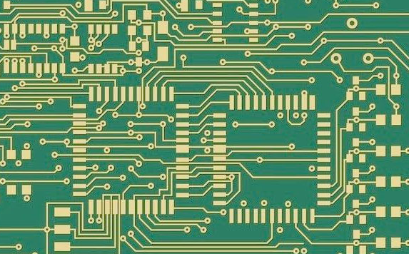
Printed Circuit Board (PCB) sub-assembly is a critical phase in the electronics manufacturing process. It involves the integration of various components onto a PCB to create a functional electronic module. This process is essential for the production of a wide range of electronic devices, from simple consumer gadgets to complex industrial machinery. The sub-assembly stage bridges the gap between the bare PCB and the final product, ensuring that all necessary components are correctly placed, soldered, and tested. This article delves into the intricacies of PCB sub-assembly, exploring its key processes, challenges, and the latest trends shaping the industry.
1. Understanding PCB Sub-Assembly
PCB sub-assembly refers to the process of populating a bare PCB with electronic components such as resistors, capacitors, integrated circuits (ICs), connectors, and other necessary parts. This process transforms a bare PCB into a functional electronic module that can be integrated into a larger system. The sub-assembly process is typically carried out after the PCB has been fabricated and before it undergoes final assembly into the end product.
The sub-assembly process can be broadly categorized into two main types:
- Through-Hole Technology (THT): In this method, components with leads are inserted into pre-drilled holes on the PCB and then soldered onto the opposite side. THT is known for its strong mechanical bonds, making it suitable for components that require high reliability and durability.
- Surface Mount Technology (SMT): SMT involves placing components directly onto the surface of the PCB. The components are then soldered using reflow soldering techniques. SMT is widely used in modern electronics due to its ability to support smaller components and higher component density, leading to more compact and lightweight designs.

2. Key Processes in PCB Sub-Assembly
The PCB sub-assembly process involves several key steps, each of which must be carefully executed to ensure the quality and functionality of the final product. These steps include:
2.1. Component Placement
Component placement is the first step in the sub-assembly process. It involves positioning the electronic components onto the PCB according to the design specifications. This step can be performed manually or using automated pick-and-place machines. Automated placement is preferred for high-volume production due to its speed and precision.
2.2. Soldering
Soldering is the process of joining the components to the PCB using solder, a metal alloy that melts at a relatively low temperature. The two primary soldering methods used in PCB sub-assembly are:
- Reflow Soldering: This method is commonly used in SMT. The PCB with placed components is passed through a reflow oven, where the solder paste is heated to form a permanent bond between the components and the PCB.
- Wave Soldering: This method is typically used for THT components. The PCB is passed over a wave of molten solder, which solders the component leads to the PCB.
2.3. Inspection and Testing
After soldering, the PCB undergoes inspection and testing to ensure that all components are correctly placed and soldered, and that the board functions as intended. Common inspection methods include:
- Visual Inspection: This involves manually or automatically inspecting the PCB for visible defects such as solder bridges, misaligned components, or missing parts.
- Automated Optical Inspection (AOI): AOI systems use cameras and image processing software to detect defects in the PCB.
- X-Ray Inspection: This method is used to inspect hidden solder joints, such as those found in Ball Grid Array (BGA) components.
- Functional Testing: This involves testing the PCB to ensure that it performs its intended function. Functional testing can range from simple power-on tests to complex system-level tests.
2.4. Cleaning
After soldering and inspection, the PCB may undergo a cleaning process to remove flux residues and other contaminants. Cleaning is essential to ensure the long-term reliability of the PCB, as contaminants can lead to corrosion or electrical shorts.
2.5. Conformal Coating
In some cases, the PCB may be coated with a protective layer, known as conformal coating, to protect it from environmental factors such as moisture, dust, and chemicals. Conformal coating also provides additional insulation and can improve the PCB’s resistance to vibration and thermal stress.
3. Challenges in PCB Sub-Assembly
Despite advances in technology, PCB sub-assembly is not without its challenges. Some of the key challenges include:
3.1. Miniaturization
As electronic devices become smaller and more compact, the components used in PCB sub-assembly are also shrinking. This trend towards miniaturization presents several challenges, including the need for more precise placement and soldering techniques, as well as the increased risk of defects such as solder bridges or tombstoning (where a component stands on one end due to uneven soldering).
3.2. Component Availability
The global electronics supply chain is complex and can be subject to disruptions, such as component shortages or delays. These disruptions can impact the PCB sub-assembly process, leading to production delays or increased costs.
3.3. Quality Control
Ensuring the quality of the PCB sub-assembly is critical to the reliability of the final product. However, maintaining consistent quality can be challenging, particularly in high-volume production environments. Defects such as solder joint failures, misaligned components, or electrical shorts can lead to product failures and costly recalls.
3.4. Environmental Regulations
The electronics industry is subject to stringent environmental regulations, such as the Restriction of Hazardous Substances (RoHS) directive, which restricts the use of certain hazardous materials in electronic products. Compliance with these regulations can add complexity to the PCB sub-assembly process, particularly in terms of material selection and waste management.
4. Trends in PCB Sub-Assembly
The PCB sub-assembly industry is constantly evolving, driven by advancements in technology and changing market demands. Some of the key trends shaping the industry include:
4.1. Automation and Industry 4.0
Automation is playing an increasingly important role in PCB sub-assembly, with the adoption of advanced robotics, machine learning, and artificial intelligence (AI) technologies. These technologies enable faster, more precise, and more efficient production processes, reducing the risk of human error and improving overall product quality.
The concept of Industry 4.0, which refers to the integration of digital technologies into manufacturing processes, is also gaining traction in the PCB sub-assembly industry. Industry 4.0 technologies, such as the Internet of Things (IoT), big data analytics, and cloud computing, enable real-time monitoring and optimization of production processes, leading to improved efficiency and reduced downtime.
4.2. Advanced Materials
The development of advanced materials is another key trend in PCB sub-assembly. New materials, such as high-performance polymers, ceramic substrates, and advanced solder alloys, are being developed to meet the demands of next-generation electronic devices. These materials offer improved thermal conductivity, electrical performance, and reliability, enabling the production of smaller, faster, and more durable electronic products.
4.3. 3D Printing
3D printing, also known as additive manufacturing, is emerging as a promising technology in PCB sub-assembly. 3D printing enables the rapid prototyping of PCBs and the production of complex, customized designs that would be difficult or impossible to achieve using traditional manufacturing methods. While 3D printing is still in its early stages in the PCB industry, it has the potential to revolutionize the way PCBs are designed and manufactured.
4.4. Green Manufacturing
As environmental concerns continue to grow, there is increasing pressure on the electronics industry to adopt more sustainable manufacturing practices. Green manufacturing initiatives, such as the use of lead-free solder, recycling of electronic waste, and the adoption of energy-efficient production processes, are becoming more prevalent in PCB sub-assembly. These initiatives not only help to reduce the environmental impact of electronic products but also align with consumer demand for more sustainable and eco-friendly products.
5. Conclusion
PCB sub-assembly is a critical stage in the electronics manufacturing process, playing a vital role in the production of functional electronic modules. The process involves several key steps, including component placement, soldering, inspection, and testing, each of which must be carefully executed to ensure the quality and reliability of the final product.
Despite the challenges posed by miniaturization, component availability, quality control, and environmental regulations, the PCB sub-assembly industry is evolving rapidly, driven by advancements in automation, materials science, and digital technologies. As the industry continues to innovate, we can expect to see further improvements in the efficiency, precision, and sustainability of PCB sub-assembly processes, enabling the production of ever more advanced and reliable electronic devices.
In conclusion, PCB sub-assembly is a complex and dynamic field that requires a deep understanding of both the technical and logistical aspects of electronics manufacturing. By staying abreast of the latest trends and technologies, manufacturers can ensure that they remain competitive in this fast-paced and ever-changing industry.


