PCB Surface Treatment: Techniques, Applications, and Future Trends
Abstract
Printed Circuit Board (PCB) surface treatment is a critical process in electronics manufacturing that ensures reliable electrical connections, protects copper traces from oxidation, and enhances solderability. With the increasing complexity of electronic devices and the demand for higher performance, selecting the appropriate surface treatment has become more important than ever. This article explores various PCB surface treatment techniques, including Hot Air Solder Leveling (HASL), Electroless Nickel Immersion Gold (ENIG), Organic Solderability Preservative (OSP), Immersion Silver, Immersion Tin, and Electrolytic Hard Gold. The advantages, disadvantages, and applications of each method are discussed, along with emerging trends in PCB surface finishing technologies.
1. Introduction
PCBs serve as the backbone of modern electronic devices, connecting components through conductive copper traces. However, exposed copper is prone to oxidation, which can degrade solderability and electrical performance. Surface treatments are applied to protect the copper and ensure reliable solder joints. The choice of surface treatment depends on factors such as cost, environmental conditions, assembly requirements, and the intended application.
This article provides an in-depth analysis of common PCB surface treatments, their properties, and their suitability for different applications.
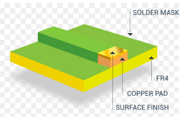
2. Common PCB Surface Treatment Techniques
2.1 Hot Air Solder Leveling (HASL)
Process: HASL involves coating the PCB with molten solder (typically tin-lead or lead-free alloys) and then using hot air to remove excess solder, leaving a flat surface.
Advantages:
- Low cost
- Excellent solderability
- Suitable for through-hole components
Disadvantages:
- Uneven surface, problematic for fine-pitch components
- Thermal shock may affect PCB reliability
- Not ideal for high-density interconnect (HDI) PCBs
Applications: Consumer electronics, industrial controls, and general-purpose PCBs.
2.2 Electroless Nickel Immersion Gold (ENIG)
Process: ENIG involves depositing a thin layer of nickel (as a diffusion barrier) followed by a thin layer of gold (to prevent oxidation).
Advantages:
- Flat surface, suitable for fine-pitch components
- Excellent oxidation resistance
- Good for wire bonding applications
Disadvantages:
- Higher cost than HASL
- Risk of “black pad” syndrome (nickel corrosion)
- Limited reworkability
Applications: High-reliability electronics, aerospace, medical devices, and RF/microwave circuits.
2.3 Organic Solderability Preservative (OSP)
Process: OSP applies a thin organic coating to protect copper from oxidation before soldering.
Advantages:
- Low cost
- Flat surface, good for fine-pitch components
- Environmentally friendly
Disadvantages:
- Limited shelf life
- Requires careful handling to avoid scratches
- Not suitable for multiple reflow cycles
Applications: Consumer electronics, computers, and telecommunications devices.
2.4 Immersion Silver (IAg)
Process: A thin layer of silver is deposited on the copper surface through a chemical displacement reaction.
Advantages:
- Good solderability
- Flat surface for fine-pitch components
- Lower cost than ENIG
Disadvantages:
- Prone to tarnishing in humid environments
- Limited shelf life compared to ENIG
Applications: High-frequency circuits, automotive electronics, and LED lighting.
2.5 Immersion Tin (ISn)
Process: A thin layer of tin is deposited on the copper surface through an immersion process.
Advantages:
- Flat surface, suitable for fine-pitch components
- Good for press-fit connectors
- Cost-effective
Disadvantages:
- Susceptible to tin whiskers (risk of short circuits)
- Limited thermal cycling resistance
Applications: Automotive electronics, power supplies, and consumer devices.
2.6 Electrolytic Hard Gold
Process: A thick layer of gold is electroplated over a nickel barrier layer.
Advantages:
- Excellent wear resistance (for connectors and switches)
- Long shelf life
- Superior corrosion resistance
Disadvantages:
- High cost
- Requires additional underplating (nickel)
Applications: Edge connectors, keypads, and high-wear applications.
3. Selection Criteria for PCB Surface Treatments
Choosing the right surface treatment depends on several factors:
- Solderability Requirements: Some treatments (HASL, ENIG) offer better solderability than others.
- Fine-Pitch Components: Flat surfaces (ENIG, OSP, IAg) are essential for high-density designs.
- Environmental Conditions: Harsh environments may require ENIG or hard gold.
- Cost Constraints: OSP and HASL are more economical than ENIG or gold plating.
- Lead-Free Compliance: Many industries require RoHS-compliant finishes (e.g., lead-free HASL, ENIG).
4. Emerging Trends in PCB Surface Treatment
4.1 Nanocoating Technologies
New nanocoatings are being developed to enhance corrosion resistance and solderability while reducing costs.
4.2 Direct Immersion Gold (DIG)
An alternative to ENIG, DIG eliminates the nickel layer, reducing the risk of black pad syndrome.
4.3 Conductive Polymers
Research is ongoing into polymer-based coatings that offer solderability without metallic layers.
4.4 Environmentally Friendly Processes
With increasing environmental regulations, manufacturers are adopting greener surface treatments, such as OSP and lead-free HASL.
5. Conclusion
PCB surface treatment is a crucial step in ensuring the reliability and performance of electronic assemblies. Each method has unique advantages and limitations, making it essential to select the right finish based on application requirements. As technology advances, new surface treatments will continue to emerge, offering improved performance, cost efficiency, and environmental sustainability.
Understanding these treatments allows engineers and manufacturers to optimize PCB designs for durability, functionality, and manufacturability in an ever-evolving electronics industry.