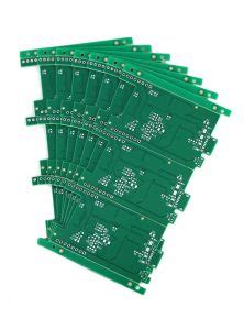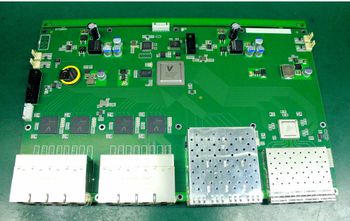
PCB technology
IN PCB design,routing is a crucial step in completing a product design.It’s a process that demands the most attention,requires the most skill,and requires the most effort.PCB routing can be performed in single-sided,double sided,or multi-layer configurations,There are two routing methods;automatic routing and interactive routing.Before automatic routing and interactive routing.Before automatic routing and interactive routing.Before automatic routing,interactive routing.Before automatic routing, interactive routing.Before automatic routing and interactive routing.Before automatic routing,interactive routing can be used to pre-route lines with more stringent requirements.Input and output edges should avoid running parallel to each other to prevent reflection interference.Ground isolation should be added when necessary.Line on adjacent layer should be perpendicular to each other;parallel to each other to prevent reflection interference. Ground isolation should be added when necessary.Lines on adjacent layers should be perpendicular to each other to prevent reflection interference.Ground isolation should be added when necessary.Lines on adjacent layers should be perpendicular to each other;parallel routing can easily lead to parasitic coupling.
The success rate of automatic routing depends on a good layout.Routing rules can be pre-set,including the number of bends,number of vias and number of steppings. routing is generally performed first to quickly connect short traces.Then,maze routing is performed,optimizing the global routing paths for the lines to be routed.Routing can also be performed as needed to disconnect already routed lines and attempt to reroute them to improve the overall result.
Through-hole routing is no longer suitable for today’s high-density PCB designs.This wastes valuable wiring channels.To address this contradiction,blind and buried via technology emerged.They not only fulfill the function of vias but also save numerous wiring channels,making the wiring process more convenient,smoother,and more complete.The PCB design process is both complex and simple.Mastering it requires the experience of electronics.
1.Power and Ground Wire Management
Even if the entire PCB is perfextly wired,interference caused by inconsiderate power and ground routing can degrade product performance and sometimes even impact product success.Therefore,careful attention must be paid to routing power and ground lines,minimizing nosie interference to ensure product quality.
Every engineer involved in electronics product design understands the cause of nosie between.Ground and power line.For now,we will only discuss noise reduction methods:
It ‘s well known that decoupling capacitors are added between the power and ground lines. Widenly increase the width of the power and ground lines.Ideally,the ground line should be wider than than the power line.Ideally,the ground line should be wider than the power line.The relationship between them is :ground>power>signal line.Typical signal line width reaching 0.05-0.07mm. Power lines are 1.2-2.5mm.
For digital circuit pcbs,wide ground conductors can be used to form a loop.This means forming a ground grid(analog circuit ground should not be used this way).Use a large copper layer as the ground line,connecting all unused areas on the printed circuit board to the ground line,Alternatively,create a multilayer board,with the power supply and ground lines occupying separate layers.
2.Common Ground Management for digital and Analog Circuits
Many PCBs now no longer consist of single-function circuist(digital or analog),but rather a mix of digital and analog circuits.Therefore,when routing,it is necessary to consider mutual interference,especially to consider mutual interference,especially noise interference,especially noise interference on the ground line.Digital circuits have high frequency signal lines should be kept as far away from sensitive For ground lines, the entire PCB has only one node to the outside world, so the digital and analog grounds must be managed internally. Internally, the digital and analog grounds are actually separate and unconnected. They only connect at interfaces (such as connectors) where the PCB connects to the outside world. Note that there is only one connection point. Some PCBs may not share a common ground; this is determined by the system design.
3.Signal Routing on the Power (Ground) Layer
When routing multilayer PCBs, there are few unfinished signal lines. Adding additional layers would result in waste, increase production workload, and increase costs. To address this issue, consider routing on the power (ground) layer. The power layer should be considered first, followed by the ground layer, as it is best to preserve the integrity of the ground layer.
4.Treatment of Connecting Legs in Large-Area Conductors
In large-area grounding (electrical) circuits, component legs are often connected to them. Treatment of connecting legs requires comprehensive consideration. From an electrical performance perspective, full contact between the component leg pads and the copper surface is optimal. However, this poses several risks to component soldering and assembly, including: ① Soldering requires a high-power heater; ② It is easy to cause cold solder joints. Therefore, considering both electrical performance and process requirements, a cross-shaped solder pad is used, known as thermal isolation. Thermal pads (also known as thermal pads) significantly reduce the possibility of cold solder joints caused by excessive heat dissipation during soldering. The power (ground) legs of multilayer boards are treated similarly.
5.The Role of the Network System in Routing
In many CAD systems, routing is determined by the network system. An overly dense grid increases the number of paths, but the step size is too small, resulting in excessive drawing data. This inevitably increases the storage space required for the device and significantly impacts the computing speed of computer-based electronic products. Some paths are ineffective, such as those occupied by component leg pads, mounting holes, or fixed-door holes. An overly sparse grid with too few paths significantly impacts routing efficiency. Therefore, a well-defined grid system is essential to support routing.
The distance between standard component legs is 0.1 inch (2.54 mm), so the grid system is generally based on a 0.1 inch (2.54 mm) grid. mm) or multiples of 0.1 inches, such as 0.05 inches, 0.025 inches, 0.02 inches, etc.
6.Design Rule Check (DRC)
After the layout design is completed, it is necessary to carefully check whether it complies with the rules established by the designer. It is also necessary to confirm whether the established rules meet the requirements of the printed circuit board production process. Generally, the following aspects should be checked:
Are the distances between lines, lines and component pads, lines and through-holes, component pads and through-holes, and through-holes reasonable and meet production requirements?
Are the widths of the power and ground lines appropriate? Are they tightly coupled (low impedance)? Is there room on the PCB for wider ground lines?
Have optimal measures been taken for critical signal lines, such as minimizing lengths, adding guard lines, and clearly separating input and output lines?
For analog and digital circuits, Have separate ground lines?
Will graphics added later to the PCB (such as icons and annotations) cause signal short circuits?
Modify any undesirable line shapes.
Are process lines added to the PCB? Does the solder mask meet production process requirements? Is the solder mask size appropriate? Are the characters and symbols pressed against the component pads to avoid affecting the quality of the electrical assembly?
Is the outer edge of the power ground layer in a multilayer board narrowed? If the copper foil of the power ground layer is exposed outside the board, it can easily cause a short circuit. Overview
The purpose of this document is to explain the PCB design process and some precautions using PowerPCB, the PCB design software from PADs. This document provides design specifications for designers working in a team, facilitating communication and mutual review.
- Design Process
The PCB design process consists of six steps: netlist input, rule setting, component placement, routing, inspection, review, and output.
2.1 Netlist Input
There are two ways to input a netlist. One is to use PowerLogic’s OLE PowerPCB Connection function. Select “Send Netlist” and apply the OLE function. This allows you to keep the schematic and PCB consistent at all times, minimizing the possibility of errors. The other method is to load the netlist directly into PowerPCB by selecting “File->Import” and importing the netlist generated from the schematic.
2.2 Rule Setting
If the PCB design rules have already been set during the schematic design phase, there is no need to set these rules again.
These rules are already imported into PowerPCB along with the netlist when the netlist is imported. If the design rules are modified, the schematic must be synchronized to ensure consistency between the schematic and PCB. In addition to design rules and layer definitions, there are other rules that need to be set, such as Pad Stacks, which require modifying the size of standard vias. If the designer creates a new pad or via, they must be added to the Layer 25.
Note:
The PCB design rules, layer definitions, via settings, and CAM output settings have been created as a default startup file named Default.stp. After importing the netlist, assign the power nets and ground planes to the power and ground planes according to the actual design, and set other advanced rules. After all rules are set, use the “Rules From PCB” function in the OLE PowerPCB Connection in PowerLogic to update the schematic rule settings to ensure consistency between the schematic and PCB layouts.
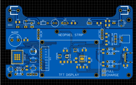
2.3 Component Placement
After importing the netlist, all components will be placed at the zero point of the workspace, overlapping them. The next step is to separate these components and arrange them neatly according to certain rules. This is known as component placement. PowerPCB provides two methods: manual placement and automatic placement. 2.3.1 Manual Placement
- Use the tool to draw the board outline using the board’s structural dimensions.
- Disperse components. Components will be arranged around the board’s edge.
- Move and rotate components one by one, placing them within the board edge and arranging them neatly according to specific rules.
2.3.2 Automatic Layout
PowerPCB provides automatic layout and automatic local cluster layout, but these are not ideal for most designs and are not recommended. 2.3.3 Notes
a. The primary principle of layout is to ensure routing efficiency. When moving components, pay attention to the connection of flying leads and place related components together.
b. Keep digital and analog components separate and as far apart as possible.
c. Place decoupling capacitors as close to the device’s VCC pin as possible.
d. When placing components, consider future soldering and avoid placing them too close together.
e. Make frequent use of the software’s Array and Union functions to improve layout efficiency.
2.4 Routing
There are two routing methods: manual routing and automatic routing. PowerPCB’s manual routing features are very powerful, including automatic pushing and shoving and online design rule checking (DRC). Automatic routing is performed by Specctra’s routing engine. These two methods are typically used in combination, with the typical steps being manual-automatic-manual.
2.4.1 Manual Routing
- Before automatic routing, manually route some important nets, such as high-frequency clocks and main power supplies. These nets often have special requirements for trace distance, width, spacing, and shielding. Special packages, such as BGAs, are difficult to route accurately with automatic routing and therefore require manual routing.
- After automatic routing, manually adjust the PCB routing.
2.4.2 Automatic Routing
After manual routing is complete, the remaining nets are routed by the autorouter. Select Tools->SPECCTRA to launch the Specctra router interface, set up the DO file, and press Continue to start the Specctra router’s automatic routing. If the routing pass rate is 100%, you can manually adjust the routing. If it is less than 100%, there is a problem with the layout or manual routing, and you need to adjust the layout or manually route until all nets are routed correctly.
2.4.3 Notes
a. Make the power and ground wires as thick as possible.
b. Connect the decoupling capacitors directly to VCC whenever possible.
c. When setting up the Specctra DO file, first add the Protect All option. Use the wires command to protect manually routed traces from being rerouted by the autorouter.
d. If there are mixed power planes, define them as Split/Mixed Planes and split them before routing. After routing, use Plane Connect in the Pour Manager to perform copper pours.
e. Set all device pins to thermal pads. To do this, set the Filter to Pins, select all pins, modify the properties, and check the Thermal option.
f. Enable DRC during manual routing and use Dynamic Route.
2.5 Verification
Check items include Clearance, Connectivity, High Speed, and Plane. These can be performed by selecting Tools->Verify Design. If High Speed is enabled, this check is mandatory; otherwise, it can be skipped. If errors are detected, the layout and routing must be revised.
Note:
Some errors can be ignored. For example, if part of the connector outline is outside the board frame, this will cause errors during the clearance check. Additionally, re-pour copper after any trace or via modification.
2.6 Review
The review is based on the “PCB Checklist” and covers design rules, layer definitions, line widths, spacing, pads, and via settings. The review also focuses on the rationality of the device layout, the routing of power and ground networks, the routing and shielding of high-speed clock networks, and the placement and connection of decoupling capacitors. If the review fails, the designer must revise the layout and routing. Upon passing, the reviewer and designer will sign off.
2.7 Design Output
PCB designs can be output to a printer or as gerber files. The printer can print the PCB in layers for easy review by the designer and reviewer. The gerber files are then handed over to the board manufacturer for production. The output of gerber files is crucial and can determine the success of the design. The following highlights the key considerations for outputting gerber files.
a. The layers that need to be output include the wiring layers (including the top, bottom, and middle wiring layers), the power layers (including the VCC and GND layers), the silkscreen layers (including the top and bottom silkscreens), the solder mask layers (including the top and bottom solder mask layers), and the generation of drill files (NC Drill).
b. If the power plane is set to Split/Mixed, select Routing from the Document section in the Add Document window. Before each output of the gerber file, use Plane Connect in the Pour Manager to copper-pour the PCB. If the power plane is set to CAM Plane, select Plane. When setting the Layer section, add Layer 25 and select Pads and Viasc in Layer 25. In the Device Setup window (press Device Setup), change the Aperture value to 199d. When setting the Layer for each layer, set the Board
Select Outline.
e. When setting the silkscreen layer, do not select Part Type. Select the Outline, Text, and Line options for the top (bottom) and silkscreen layers.
f. When setting the solder mask layer, select Via for no solder mask on the vias; unselecting Via for no solder mask. The decision depends on the specific situation.
g. When generating drill files, use the default settings in PowerPCB and do not make any changes.
h. After all gerber files are exported, open and print them in CAM350. The designer and reviewer will check them according to the “PCB Checklist.”
Vias are a crucial component of multilayer PCBs, and drilling costs typically account for 30% to 40% of the PCB fabrication cost. Simply put, every hole on a PCB can be called a via. Based on their function, vias can be divided into two categories: one for electrical connection between layers; the other for securing or positioning components. Based on the manufacturing process, these vias are generally divided into three categories: blind vias, buried vias, and through holes. Blind vias are located on the top and bottom surfaces of a printed circuit board (PCB). They are deep and connect the surface circuitry to the underlying inner layers. The hole depth typically does not exceed a certain ratio (hole diameter). Buried vias are connection holes located on the inner layers of a PCB and do not extend to the board’s surface. Both of these types of vias are located on the inner layers of the PCB and are formed using a through-hole forming process before lamination. The via formation process may also overlap several inner layers. The third type, called a through-hole, passes through the entire PCB and can be used for internal interconnects or as mounting holes for components. Because through-holes are easier to create and less expensive, they are used in most PCBs instead of the other two types of vias. Unless otherwise specified, all vias mentioned below are considered through-holes.
From a design perspective, a via consists of two main components: a central drill hole (drill hole). The first is the via hole, and the second is the pad area surrounding the drilled hole, as shown in the figure below. The dimensions of these two components determine the size of the via. Obviously, in high-speed, high-density PCB design, designers always prefer to keep vias as small as possible to allow for more wiring space on the board. Furthermore, smaller vias reduce their inherent parasitic capacitance, making them more suitable for high-speed circuits. However, reducing via size also increases costs, and via size cannot be reduced indefinitely due to process limitations such as drilling and plating. Smaller holes require longer drilling times and are more likely to be off-center. Furthermore, when the hole depth exceeds six times the drilled hole diameter, uniform copper plating cannot be guaranteed on the hole walls. For example, the thickness (through-hole depth) of a typical six-layer PCB is currently around 50 mils, so PCB manufacturers can only offer drilled holes with a minimum diameter of 8 mils.
II. Parasitic Capacitance of Vias
Vias inherently have parasitic capacitance to ground. For capacitance, if the via’s isolation hole diameter on the ground plane is D2, the via pad’s diameter is D1, the PCB thickness is T, and the substrate’s dielectric constant is ε, then the via’s parasitic capacitance is approximately:
C = 1.41εTD1/(D2 – D1)
The primary impact of via parasitic capacitance on a circuit is that it prolongs the signal’s rise time, reducing circuit speed. For example, for a 50-mil thick PCB, if a 10-mil inner diameter via is used… , the pad diameter of the via is 20 mil, and the distance between the pad and the ground copper area is 32 mil. Then we can use the above formula to approximately calculate the parasitic capacitance of the via: C = 1.41×4.4×0.050×0.020/(0.032-0.020) = 0.517pF. The rise time change caused by this part of the capacitance is: T10-90 = 2.2C(Z0/2) = 2.2×0.517x(55/2) = 31.28ps These values show that while the effect of a single via’s parasitic capacitance on slowing the rise time is not significant, designers should still carefully consider it if multiple vias are used for interlayer switching.
3.Via Parasitic Inductance
Similarly, vias have both parasitic capacitance and inductance. In high-speed digital circuit design, the parasitic inductance of a via often poses a greater risk than the parasitic capacitance. Its parasitic series inductance weakens the contribution of the bypass capacitor and reduces the filtering effectiveness of the entire power supply system. We can use the following formula to simply calculate the approximate parasitic inductance of a via:
L = 5.08h [ln(4h/d) + 1], where L is the via inductance, h is the via length, and d is the diameter of the center hole. As can be seen from the formula, the via diameter has a minor impact on the inductance, while the via length has the greatest influence. Using the same example as above, the via inductance can be calculated as: L = 5.08 x 0.050 [ln(4 x 0.050/0.010) + 1] = 1.015nH. If the signal rise time is 1ns, then its equivalent impedance is: XL = πL / T10 – 90 = 3.19Ω. This impedance is not negligible when high-frequency currents are flowing. In particular, the bypass capacitor needs to pass through two vias when connecting the power and ground planes, which multiplies the parasitic inductance of the vias.
4. Via Design in High-Speed PCBs
The above analysis of via parasitic characteristics shows that in high-speed PCB design, seemingly simple vias can often have significant negative effects on circuit design. To minimize the adverse effects of via parasitics, the following should be considered in the design:
Place ground vias near signal vias that switch layers to provide the closest possible return path for the signal. You can even place a large number of redundant ground vias on the PCB. Of course, flexibility is required in design. The via model discussed above assumes that every layer has a pad. Sometimes, the pads on certain layers can be reduced or even eliminated. Especially when the via density is very high, this can lead to a broken path in the copper layer, which can interrupt the return path. To address this problem, in addition to moving the vias, you can also consider reducing the pad size of the via on that copper layer.
Consider both cost and signal quality when selecting a reasonable via size. For example, for a 6-10 layer memory module PCB, 10/20 mil (drill/pad) vias are preferred. For smaller, high-density boards, 8/18 mil vias can also be used. Current technology makes it difficult to use smaller via sizes. For power or ground vias, Consider using larger vias to reduce impedance.
The two formulas discussed above indicate that using thinner PCBs helps reduce the two parasitic parameters of vias.
Signal traces on the PCB should avoid switching layers as much as possible, which means avoiding unnecessary vias.
Power and ground vias should be placed close to the pins. The traces between the vias and the pins should be as short as possible, as they increase inductance. Power and ground traces should also be as thick as possible to reduce impedance.