PCB technology is developing well. Will you make these mistakes during the design process?
In terms of the current status and trends of international electronic circuits, the development prospects of PCB are very broad, but we will inevitably encounter some mistakes during the design process. This article will take you to see the development prospects of PCB and several common mistakes. Will you make these mistakes? Knowing these mistakes before they affect the overall function of the circuit board is a good way to avoid costly production delays.

First, let’s look at the development prospects and trends of PCB:
1.Chip-scale packaging CSP will gradually replace TSOP and ordinary BGA
CSP is a chip-scale package. It is not a separate package form, but a chip-scale package when the chip area and package area can be compared. CSP packaging can make the ratio of chip area to package area exceed 1:1.14, which is quite close to the ideal situation of 1:1, and is about 1/3 of ordinary BGA; the central pin form of CSP packaged chips effectively shortens the transmission distance of signals, and its attenuation is reduced accordingly, and the anti-interference and anti-noise performance of chips can also be greatly improved. In the CSP packaging method, chip particles are soldered on the PCB board through solder balls one by one. Due to the large contact area between the solder joints and the PCB board, the heat generated by the chip during operation can be easily conducted to the PCB board and dissipated.
Development prospects: Chip-level packaging developed in response to the light, thin, short and small electronic products is a new generation of packaging. According to the development trend of electronic products, chip-level packaging will continue to develop rapidly and gradually replace TSOP (Thin Small Outline Package) packaging and ordinary BGA packaging.
2.By 2010, the output value of photovoltaic panels will increase by 14% annually
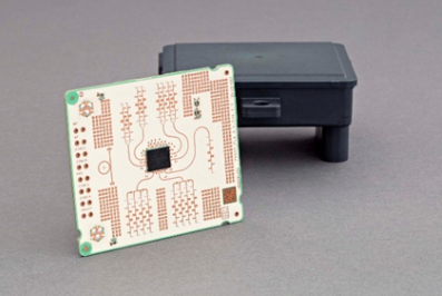
Photoelectric panels, also known as photovoltaic backplanes, are a special printed circuit board with built-in optical channels. It is also a type of backplane and is mainly used in the communication field. The main advantages of optoelectronic backplanes: low signal distortion; avoid noise; very low crosstalk; loss is independent of frequency; dense wavelength multi-way splitting technology; 12-6 channel multi-way connectors; waveguide multi-channel connectors; improve the reliability of discrete cables; optoelectronic boards can have up to 20 layers, more than 20,000 lines, and 1,000 pins in connectors; the bandwidth of traditional backplanes is limited to a certain extent due to the use of copper wires.
Development prospects: Due to the increase in bandwidth and distance, the transmission line of copper materials will reach the limit of bandwidth and distance, while optoelectronic transmission can meet the needs of increased bandwidth and distance. Optoelectronic backplanes are mainly used in communication exchange and data exchange, and will be applied to workstations and servers in the future. According to forecasts, the global output value of optoelectronic backplanes will reach US$200 million by 2010, with an annual growth of about 14%.
3.The development prospects of rigid-flexible boards are very promising
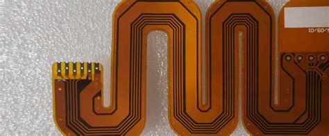
Flexible boards FPC used to be called very confusingly. They were first called soft boards, and later they were called flexible boards, flexible printed circuit boards, etc.
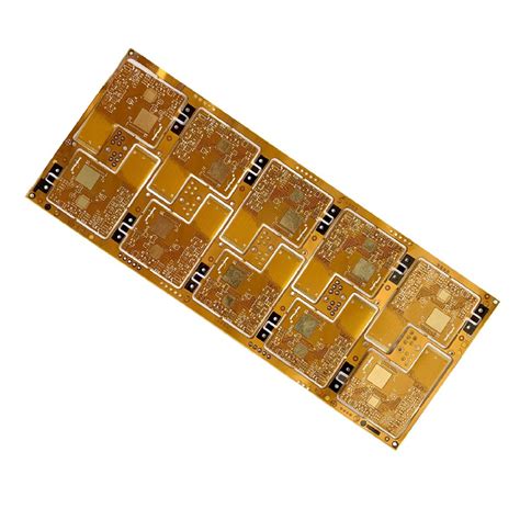
Rigid-flex PCB refers to a PCB containing one or more rigid areas and one or more flexible areas. It is composed of rigid boards and flexible boards laminated together in an orderly manner, and the electrical connection is formed by metallized holes. Rigid-flex PCB can provide both the support that rigid PCB should have and the bendability of flexible boards. It can meet the requirements of three-dimensional assembly and has been in increasing demand in recent years. The design concept of traditional rigid-flex PCB is to save space, facilitate assembly and improve reliability; the new rigid-flex PCB that combines traditional rigid-flex PCB design and micro blind hole technology provides a new solution for the interconnection field. Its advantages are: suitable for folding mechanisms, such as flip phones, cameras, and laptops; improve product reliability; apply traditional assembly methods, but simplify assembly and make it suitable for 3D assembly; combine with micro-pipe technology to provide better design convenience and use smaller components; use lighter materials instead of traditional FR-4.
Rigid-flex PCBs used in mobile phones are generally made of two layers of flexible boards connected to hard boards.
Development prospects: Rigid-flex boards are a type of PCB that has grown very rapidly in recent years. They are widely used in computers, aerospace, military electronic equipment, mobile phones, digital (cameras), communication equipment, analytical instruments, etc. It is predicted that the average annual growth rate from 2005 to 2010 will exceed 20% in terms of output value, and the average annual growth rate in terms of area will exceed 37%, which greatly exceeds the growth rate of ordinary PCBs. So far, there are very few manufacturers that can produce rigid-flex boards, and almost no manufacturers have experience in mass production, so its development prospects are very promising.
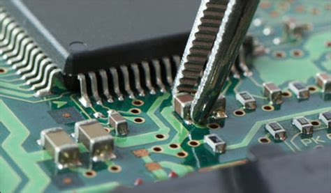
4.High-layer boards bring opportunities to the Chinese industry
Multilayer boards refer to PCB boards with independent wiring layers greater than two layers. They are generally composed of multiple double-sided boards laminated together, and each layer of boards is laminated into a whole board through an insulating layer. High-layer boards generally refer to multilayer boards with more than 10 layers, which are mainly used in switches, routers, servers and large computers. Some supercomputers use more than 40 layers.
Development prospects: Ordinary multilayer boards are mature products, and the future growth is relatively stable; however, high-layer boards have high technical content, and the fact that Europe and the United States have basically abandoned conventional PCB production has brought some opportunities to the Chinese industry. It is predicted that the annual growth rate of high-layer boards (backplanes) will be about 13% in the future.
5. 3G boards improve the technical level of PCB products
Printed boards adapted to the third-generation mobile communication products (3G). 3G boards generally refer to 3G mobile phone boards. It is a high-end printed circuit board manufactured using advanced secondary lamination technology with a line grade of 3mil (75μm). The technologies involved include electroplating hole filling, stacking holes, rigid-flex integration, and a series of cutting-edge printed circuit board technologies. 3G technology is significantly improved over existing products.
Development prospects: 3G is the next generation of mobile communication technology. Currently, developed countries such as Europe, the United States and Japan have begun to apply it. 3G will eventually replace the existing 2G and 2.5G communications. By the end of 2005, the number of global 3G users increased by 57.4%, and the total number has reached 237 million. In 2005, a total of 122 million 3G mobile phones of various formats were sold. The future development will still maintain a growth rate of more than 20%. The matching printed circuit board, namely the 3G board, maintains the same growth rate. The 3G board is an upgrade of the existing products, which makes the overall level of the PCB industry step into a higher level.
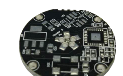
6.HDI board will grow rapidly in the future
HDI is the abbreviation of High Density Interconnect, which is a (technology) for producing printed circuit boards. It is currently widely used in mobile phones, digital (cameras), MP3, MP4, etc. It is generally manufactured by build-up. The more times the build-up is, the higher the technical level of the board. Ordinary HDI boards are basically 1-time stacking, while high-order HDI uses 2 or more stacking technologies, and also uses advanced PCB technologies such as stacking holes, electroplating filling holes, and laser direct drilling. High-order HDI boards are mainly used in 3G mobile phones, advanced digital cameras, IC carrier boards, etc.
Development prospects: According to the use of high-order HDI boards-3G boards or IC carrier boards, its future growth is very rapid: the world’s 3G mobile phone growth will exceed 30% in the next few years, and China is about to issue 3G licenses; IC carrier industry consulting agency Prismark predicts that China’s forecast growth rate from 2005 to 2010 is 80%, which represents the technical development direction of PCB.
Development is indeed fast, but the errors we will encounter during design are as follows:
1.) Landing pattern
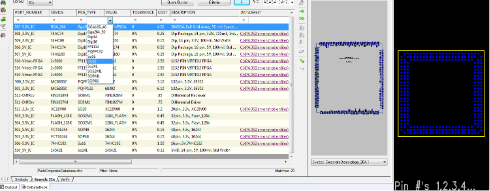
Although most PCB design software includes a library of general electrical components, their associated schematic symbols, and landing patterns, some circuit boards will require designers to draw them manually. If the error is less than half a millimeter, engineers must be very strict to ensure the proper spacing between pads. Mistakes made in this production stage will make soldering difficult or impossible. Necessary rework will result in costly delays.
2.) Use of Blind/Buried Vias
In a market where devices are now used to IoT, smaller and smaller products continue to have the greatest impact. When smaller devices require smaller PCBs, many engineers choose to reduce the footprint of the board by utilizing blind and buried vias to connect internal and external layers. Although vias can effectively reduce the area of the PCB, they reduce the routing space and can become complicated as the number of vias added increases, making some boards expensive and unmanufacturable.
3.) Trace Width
In order to make the board size small and compact, engineers aim to make the traces as narrow as possible. There are many variables involved in determining the PCB trace width, which makes it difficult, so it is necessary to have a comprehensive understanding of how much milliamps will be required. In most cases, the minimum width requirement is not enough. We recommend using a width calculator to determine the appropriate thickness and ensure design accuracy.
Opportunities are also challenges, and we should take my opportunities and avoid mistakes.

