PCB Tenting Vias: A Comprehensive Guide to Design, Benefits, and Manufacturing Considerations
Introduction to Via Tenting in PCB Design
Printed Circuit Board (PCB) design has evolved significantly over the past few decades, with via tenting emerging as one of the most important techniques for modern electronic assemblies. Via tenting refers to the process of covering the annular rings and openings of vias with solder mask material, creating a protective layer that shields these critical interconnects from environmental factors and potential solder bridging during assembly.
As electronic devices continue to shrink in size while increasing in complexity, proper via treatment has become essential for reliable PCB performance. Tenting vias offers numerous advantages over alternative via treatments, particularly in high-density designs where space is at a premium and reliability cannot be compromised.
This article will provide a comprehensive examination of PCB via tenting, exploring its technical aspects, design considerations, manufacturing processes, and the various benefits it offers to modern electronics. We’ll also compare tenting with other via protection methods and discuss specific applications where tented vias provide the most value.
Understanding PCB Vias and Their Functions
Before delving into tenting specifically, it’s crucial to understand the fundamental role of vias in PCB architecture. Vias are conductive pathways that connect different layers of a multilayer PCB, allowing electrical signals and power to travel between layers. These small holes, typically plated with copper, serve as the vertical interconnects in what is otherwise a horizontal circuit layout.
Types of PCB Vias
- Through-hole vias: These extend through the entire thickness of the PCB, connecting all layers from top to bottom.
- Blind vias: These connect an outer layer to one or more inner layers but do not pass through the entire board.
- Buried vias: These connect inner layers only and are not visible from either surface of the PCB.
- Microvias: These are small vias (typically less than 150μm in diameter) often used in high-density interconnect (HDI) designs.
Each via type presents unique considerations for tenting, with through-hole vias being the most commonly tented in standard PCB designs.
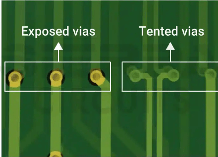
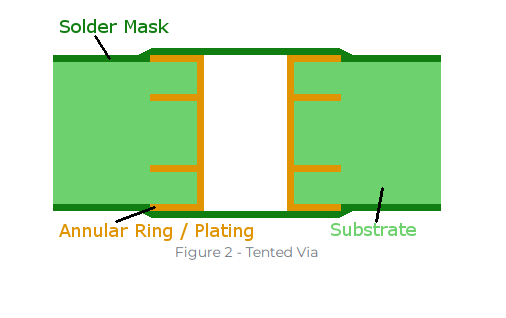
What is Via Tenting?
Via tenting is a solder mask application technique where the solder mask material completely covers the via’s annular ring and its opening. This creates a protective barrier that:
- Prevents solder and other contaminants from entering the via during assembly
- Reduces the risk of solder bridging between nearby vias or components
- Provides environmental protection against moisture and corrosive elements
- Improves the board’s aesthetic appearance by creating a uniform surface
The tenting process occurs during PCB manufacturing, typically after the copper plating stage but before surface finishing. The solder mask is applied over the entire board surface, including the via openings, and then cured to create a durable protective layer.
Benefits of Tenting Vias
1. Enhanced Reliability and Protection
Tented vias offer superior protection against environmental factors that could compromise PCB performance:
- Moisture resistance: By sealing the via opening, tenting prevents moisture ingress that could lead to oxidation or electrochemical migration.
- Contaminant barrier: The solder mask blocks dust, flux residues, and other contaminants from entering the via barrel.
- Mechanical protection: The mask layer adds structural support to the via area, reducing the risk of damage during handling or assembly.
2. Improved Solderability and Assembly Yield
During the soldering process, tented vias provide several advantages:
- Prevents solder wicking: Without tenting, molten solder can flow into vias through capillary action, potentially starving nearby joints of solder.
- Reduces solder bridging: The solder mask acts as a physical barrier between adjacent vias and pads, minimizing the risk of unintended connections.
- Eliminates solder balls: Open vias can trap flux gases during reflow, potentially causing solder ball formation when the gas escapes.
3. Space Optimization and Design Flexibility
Tenting enables more efficient use of PCB real estate:
- Allows for via-in-pad designs where vias are placed directly under component pads
- Enables higher routing density by reducing keep-out areas around vias
- Facilitates the use of smaller via sizes without compromising reliability
4. Electrical Performance Benefits
While often overlooked, tented vias can improve certain electrical characteristics:
- Reduced parasitic capacitance between closely spaced vias
- Minimized risk of electromagnetic interference (EMI) from via openings
- Better controlled impedance by providing more consistent dielectric environments
Design Considerations for Tented Vias
Successful implementation of via tenting requires careful attention to several design parameters:
1. Via Size and Aspect Ratio
The ability to effectively tent a via depends largely on its dimensions:
- Diameter: Smaller vias (especially those below 0.3mm) tent more reliably than larger ones
- Aspect ratio: The ratio of via depth to diameter affects how well solder mask can cover the opening
- Annular ring: Adequate copper padding around the via hole ensures proper mask adhesion
2. Solder Mask Material and Thickness
Different solder mask formulations have varying tenting capabilities:
- Liquid photoimageable solder masks (LPSM): Most common, good for small to medium vias
- Dry film solder masks: Offer more consistent thickness but may have limitations with very small vias
- Specialty high-build masks: Designed specifically for reliable tenting of larger vias
3. Board Layout and Via Placement
Strategic via placement enhances tenting success:
- Maintain adequate spacing between vias to ensure complete mask coverage
- Avoid placing vias too close to board edges where mask application may be inconsistent
- Consider via grouping patterns that facilitate uniform mask application
4. Manufacturing Process Requirements
Designers must account for fabrication capabilities:
- Different PCB manufacturers may have varying tenting capabilities and preferences
- Some processes may require specific via size limitations for reliable tenting
- Certain surface finishes may interact differently with tented vias
Manufacturing Process for Tented Vias
The production of PCBs with tented vias follows a specific sequence:
- Drilling: Vias are drilled or laser-ablated according to design specifications
- Plating: Copper is deposited to form conductive barrels in the via holes
- Solder mask application: Liquid or dry film mask is applied to the entire board surface
- Exposure and development: The mask is patterned using photolithography techniques
- Curing: The solder mask is hardened through thermal or UV curing processes
- Surface finishing: Final coatings (ENIG, HASL, OSP, etc.) are applied as needed
Key factors affecting tenting quality in manufacturing include:
- Solder mask viscosity and surface tension properties
- Application method (curtain coating, spray coating, or screen printing)
- Curing parameters (temperature, duration, and atmosphere)
- Equipment precision and process control
Comparison with Other Via Protection Methods
While tenting is popular, it’s not the only via protection option available:
1. Tenting vs. Via Plugging
Via plugging involves filling the via completely with a non-conductive or conductive material:
- Provides more complete protection than tenting
- Allows for via-in-pad implementations
- More expensive and time-consuming process
- Often used for high-reliability or thermal management applications
2. Tenting vs. Via Capping
Via capping builds upon plugging by adding a planar surface:
- Creates an entirely flat surface for component placement
- Essential for some advanced packaging technologies
- Significant additional cost over basic tenting
3. Tenting vs. Open Vias
Leaving vias completely uncovered:
- Lowest cost option
- Maximum exposure to environmental risks
- Potential for solder-related issues during assembly
- Sometimes used for test points or thermal vias
Challenges and Limitations of Via Tenting
While tenting offers numerous benefits, designers should be aware of its potential drawbacks:
- Tenting reliability: For larger vias, the solder mask may form a thin membrane that could rupture during thermal cycling or mechanical stress.
- Gas entrapment: During soldering, trapped gases in tented vias can cause localized pressure buildup, potentially leading to mask blistering or delamination.
- Inspection difficulties: Tented vias make it harder to visually inspect the via barrel for plating quality or other defects.
- Thermal considerations: The solder mask adds an extra layer of insulation that may slightly affect heat dissipation in thermal vias.
- Process variability: Tenting quality can vary between manufacturers and even between batches, requiring careful supplier qualification.
Best Practices for Designing with Tented Vias
To maximize the benefits of via tenting while minimizing potential issues, follow these guidelines:
- Consult with your manufacturer early: Understand their specific capabilities and limitations regarding via tenting.
- Standardize via sizes: Use consistent via dimensions across the design to ensure uniform tenting.
- Maintain proper clearances: Ensure adequate spacing between tented vias and nearby features.
- Consider via placement: Avoid placing tented vias in high-stress areas or locations prone to mechanical contact.
- Specify tenting requirements clearly: Include detailed tenting specifications in your fabrication notes.
- Balance tenting with testability: Leave some vias open if electrical testing access is required.
- Review thermal needs: Evaluate whether critical thermal vias should be left open or treated differently.
Advanced Applications of Tented Vias
As PCB technology advances, tented vias find use in increasingly sophisticated applications:
1. High-Density Interconnect (HDI) Designs
In HDI boards with microvias and dense routing, tenting:
- Enables via-in-pad configurations
- Allows for finer pitch components
- Reduces crosstalk between closely spaced vias
2. Flexible and Rigid-Flex PCBs
For flexible circuits, tenting:
- Provides additional mechanical support to via structures
- Helps maintain flexibility by preventing crack propagation
- Protects vias in dynamic bending areas
3. High-Frequency RF/Microwave Boards
In RF applications, tented vias:
- Provide more consistent dielectric properties
- Reduce unwanted radiation from via openings
- Enable better impedance control
4. Automotive and Aerospace Electronics
For harsh environment applications, tenting:
- Enhances resistance to vibration and thermal cycling
- Protects against moisture and chemical exposure
- Meets stringent reliability requirements
Future Trends in Via Tenting Technology
The evolution of PCB technology continues to drive innovations in via tenting:
- Improved solder mask materials: New formulations with better tenting reliability and durability.
- Laser-assisted tenting: Precision laser techniques for more consistent via coverage.
- Nanocomposite masks: Incorporation of nanoparticles for enhanced mechanical and thermal properties.
- Adaptive tenting processes: Smart manufacturing approaches that adjust parameters based on via characteristics.
- 3D-printed solder masks: Additive manufacturing techniques for customized via protection.
Conclusion
PCB via tenting has established itself as an essential technique in modern electronics manufacturing, offering an optimal balance of protection, reliability, and cost-effectiveness for most applications. By understanding the principles, benefits, and limitations of via tenting, designers can make informed decisions that enhance their PCB’s performance and manufacturability.
As electronic devices continue to push the boundaries of miniaturization and functionality, the proper implementation of via tenting will remain a critical factor in successful PCB design. By following best practices and staying informed about manufacturing capabilities, engineers can leverage tented vias to create robust, high-performance electronic products that meet the demanding requirements of today’s markets.
Whether working on consumer electronics, automotive systems, or advanced aerospace applications, a thorough understanding of via tenting principles empowers designers to make the most of this valuable PCB technology while avoiding common pitfalls. As with all aspects of PCB design, collaboration with experienced manufacturing partners and careful attention to detail will ensure the best results when implementing tented vias in your next project.