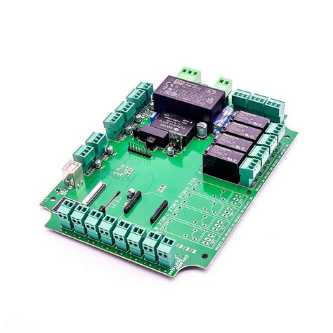
Pcb terminals connectors for high frequency and high current
Innovations In PCB Terminal Connectors For High-Frequency Applications
Printed Circuit Board (PCB) terminal connectors have undergone significant advancements to meet the demands of high-frequency and high-current applications. As electronic devices become more sophisticated, the need for reliable and efficient connectors has never been more critical. These connectors serve as the lifeline for transmitting signals and power between different components on a PCB, and their performance directly impacts the overall functionality of the device.
One of the primary challenges in designing PCB terminal connectors for high-frequency applications is minimizing signal loss and interference.
High-frequency signals are particularly susceptible to attenuation and electromagnetic interference (EMI), which can degrade signal integrity. To address this, manufacturers have developed connectors with advanced shielding techniques and materials that reduce EMI. For instance, connectors with metalized housings and ground planes can effectively shield sensitive signals from external noise, ensuring that the signal remains clean and undistorted.
In addition to shielding, the geometry and materials of the connectors play a crucial role in their performance.
High-frequency connectors often feature precision-engineered contacts made from materials with excellent conductivity, such as gold or silver. These materials not only provide low resistance paths for the signals but also offer superior corrosion resistance, which is essential for maintaining long-term reliability. Furthermore, the use of dielectric materials with low permittivity in the connector design helps to minimize signal loss and maintain high signal integrity.
Transitioning to high-current applications, the focus shifts to the ability of the connectors to handle large amounts of power without overheating or causing voltage drops.
High-current connectors are designed with robust contact points and larger cross-sectional areas to accommodate higher current flows. The use of materials with high thermal conductivity, such as copper alloys, helps to dissipate heat efficiently, preventing thermal buildup that could damage the connector or the PCB.
Moreover, the mechanical design of high-current connectors is critical to their performance.
These connectors often feature secure locking mechanisms and robust housings to ensure a stable and reliable connection, even in environments subject to vibration or mechanical stress. The use of spring-loaded contacts or screw terminals can provide additional contact force, ensuring a low-resistance connection that can handle high currents without significant voltage drops.
Another innovation in PCB terminal connectors is the integration of smart features that enhance their functionality and reliability.
For example, some connectors now come with built-in sensors that monitor temperature and current flow, providing real-time data that can be used to prevent overheating and ensure optimal performance. These smart connectors can communicate with the device’s control system, enabling predictive maintenance and reducing the risk of unexpected failures.
As the demand for high-frequency and high-current applications continues to grow, the development of advanced PCB terminal connectors will remain a critical area of focus.
Innovations in materials, design, and smart features are driving the evolution of these connectors, ensuring that they can meet the stringent requirements of modern electronic devices. By addressing the challenges of signal integrity, thermal management, and mechanical stability, these advanced connectors are paving the way for more reliable and efficient electronic systems.
In conclusion, the advancements in PCB terminal connectors for high-frequency and high-current applications are a testament to the ongoing innovation in the field of electronics. As technology continues to evolve, these connectors will play an increasingly vital role in ensuring the performance and reliability of electronic devices, making them indispensable components in the ever-expanding world of high-tech applications.
Optimizing High-Current PCB Terminal Connectors For Enhanced Performance
In the realm of modern electronics, the demand for high-frequency and high-current applications has surged, necessitating the development of advanced PCB terminal connectors. These connectors play a pivotal role in ensuring the efficient transmission of electrical signals and power, thereby enhancing the overall performance of electronic devices. To optimize these connectors for high-current applications, several critical factors must be considered, including material selection, design intricacies, and thermal management.
Firstly, the choice of materials is paramount in the development of high-current PCB terminal connectors.
Conductive materials such as copper and its alloys are often preferred due to their excellent electrical conductivity and thermal properties. Copper, in particular, offers low electrical resistance, which is crucial for minimizing power loss and ensuring efficient current flow. Additionally, the use of high-quality insulating materials is essential to prevent short circuits and maintain the integrity of the electrical connections. These materials must exhibit high dielectric strength and thermal stability to withstand the demanding conditions of high-frequency and high-current applications.
Transitioning to the design aspects, the geometry and layout of PCB terminal connectors significantly influence their performance.
The connectors must be designed to minimize inductance and resistance, which can cause signal degradation and power loss. This can be achieved through the use of wide and thick traces, as well as the incorporation of multiple layers in the PCB design. Furthermore, the connectors should be strategically placed to reduce the length of current paths and minimize electromagnetic interference (EMI). Proper spacing between connectors is also crucial to prevent crosstalk and ensure reliable signal transmission.
Thermal management is another critical consideration in optimizing high-current PCB terminal connectors.
High-current applications generate substantial heat, which can adversely affect the performance and longevity of electronic components. Effective thermal management strategies, such as the use of heat sinks, thermal vias, and conductive cooling materials, are essential to dissipate heat and maintain optimal operating temperatures. Additionally, the implementation of thermal simulation tools during the design phase can help identify potential hotspots and optimize the thermal performance of the connectors.
Moreover, the mechanical robustness of PCB terminal connectors is vital for ensuring reliable performance in high-current applications.
The connectors must be able to withstand mechanical stresses, such as vibrations and shocks, without compromising their electrical integrity. This can be achieved through the use of robust connector housings and secure mounting mechanisms. Additionally, the connectors should be designed to facilitate easy assembly and disassembly, allowing for efficient maintenance and repair.
In conclusion, optimizing high-current PCB terminal connectors for enhanced performance requires a comprehensive approach that encompasses material selection, design optimization, thermal management, and mechanical robustness. By carefully considering these factors, engineers can develop connectors that not only meet the demanding requirements of high-frequency and high-current applications but also ensure reliable and efficient operation. As the demand for advanced electronic devices continues to grow, the development of optimized PCB terminal connectors will play a crucial role in driving innovation and enhancing the performance of modern electronics
Challenges And Solutions In Designing High-Frequency PCB Terminal Connectors
Designing high-frequency PCB terminal connectors presents a unique set of challenges that require innovative solutions to ensure optimal performance. As electronic devices become more sophisticated, the demand for connectors that can handle high frequencies and high currents has surged. This necessitates a deep understanding of the underlying principles and potential pitfalls associated with such designs.
One of the primary challenges in designing high-frequency PCB terminal connectors is managing signal integrity.
High-frequency signals are particularly susceptible to interference and signal degradation, which can lead to data loss or corruption. To mitigate these issues, designers must carefully consider the materials and geometries used in the connectors. For instance, using low-loss dielectric materials can help maintain signal integrity by reducing signal attenuation. Additionally, the physical layout of the connectors, including the spacing and alignment of the pins, plays a crucial role in minimizing crosstalk and electromagnetic interference (EMI).
Another significant challenge is thermal management.
High-current applications generate substantial amounts of heat, which can adversely affect the performance and longevity of the connectors. Effective thermal management strategies are essential to dissipate heat and prevent overheating. This can be achieved through the use of materials with high thermal conductivity, such as copper or aluminum, and incorporating heat sinks or thermal vias into the PCB design. Moreover, optimizing the connector’s design to ensure efficient airflow can further enhance heat dissipation.
Mechanical reliability is also a critical consideration in the design of high-frequency PCB terminal connectors.
These connectors must withstand mechanical stresses, such as vibrations and shocks, without compromising their electrical performance. To address this, designers often employ robust materials and construction techniques. For example, using gold-plated contacts can enhance durability and reduce the risk of corrosion, ensuring a reliable connection over time. Additionally, incorporating strain relief features can help distribute mechanical stresses more evenly, reducing the likelihood of connector failure.
The miniaturization of electronic devices adds another layer of complexity to the design of high-frequency PCB terminal connectors.
As devices become smaller, the available space for connectors is significantly reduced, necessitating more compact and efficient designs. This often involves the use of advanced manufacturing techniques, such as micro-molding and precision stamping, to produce connectors with fine pitch and high pin density. Furthermore, designers must ensure that these miniaturized connectors can still handle the required current levels without overheating or experiencing excessive voltage drops.
To address these challenges, collaboration between different engineering disciplines is essential.
Electrical engineers, mechanical engineers, and materials scientists must work together to develop comprehensive solutions that address the multifaceted nature of high-frequency PCB terminal connector design. This interdisciplinary approach enables the integration of advanced materials, innovative thermal management techniques, and robust mechanical designs to create connectors that meet the stringent requirements of modern electronic devices.
In conclusion, designing high-frequency PCB terminal connectors for high-current applications involves navigating a complex landscape of challenges. By focusing on signal integrity, thermal management, mechanical reliability, and miniaturization, designers can develop connectors that deliver exceptional performance and reliability. Through interdisciplinary collaboration and the application of advanced technologies, the industry can continue to push the boundaries of what is possible, enabling the next generation of high-performance electronic devices..
Material Selection For High-Current PCB Terminal Connectors: Best Practices
When designing high-current PCB terminal connectors, the selection of materials is a critical factor that significantly influences performance, reliability, and longevity. The materials chosen must withstand the electrical, thermal, and mechanical stresses inherent in high-frequency and high-current applications. To ensure optimal performance, several best practices should be followed in the material selection process.
Firstly, the conductive materials used in the connectors must exhibit excellent electrical conductivity to minimize resistive losses and ensure efficient current flow.
Copper and its alloys are commonly preferred due to their superior conductivity and relatively low cost. However, for applications requiring even higher performance, silver or gold plating may be employed to further reduce contact resistance and enhance corrosion resistance. The choice between these materials often hinges on a balance between performance requirements and budget constraints.
In addition to electrical conductivity, thermal management is a paramount consideration.
High-current applications generate significant heat, which must be effectively dissipated to prevent overheating and potential failure. Materials with high thermal conductivity, such as copper, are advantageous in this regard. Furthermore, the use of thermal interface materials (TIMs) can enhance heat dissipation by improving the thermal coupling between the connector and the PCB. These TIMs, often composed of thermally conductive polymers or ceramics, help to spread heat more evenly and reduce thermal hotspots.
Mechanical robustness is another crucial factor in material selection.
High-current connectors must endure mechanical stresses from insertion and extraction cycles, as well as potential vibrations and shocks during operation. Materials with high tensile strength and fatigue resistance, such as beryllium copper or phosphor bronze, are often employed to ensure long-term mechanical reliability. Additionally, the use of robust housing materials, such as high-performance thermoplastics or metal alloys, can provide added protection and durability.
Corrosion resistance is also essential, particularly in harsh environments where exposure to moisture, chemicals, or other corrosive agents is likely.
Corrosion can degrade the electrical and mechanical properties of the connectors, leading to increased resistance, heat generation, and potential failure. To mitigate this risk, materials with inherent corrosion resistance, such as stainless steel or nickel-plated surfaces, are often utilized. In some cases, additional protective coatings or sealants may be applied to further enhance corrosion resistance.
Moreover, the compatibility of the chosen materials with the PCB substrate and other components must be carefully considered.
Mismatched coefficients of thermal expansion (CTE) between the connector materials and the PCB can lead to mechanical stresses and potential failure during thermal cycling. Therefore, selecting materials with compatible CTE values is crucial to maintaining the integrity of the connections over a wide temperature range.
Finally, manufacturability and cost-effectiveness are practical considerations that cannot be overlooked.
While high-performance materials may offer superior properties, they often come at a higher cost and may present manufacturing challenges. Balancing performance requirements with cost constraints is essential to achieving a viable and economically feasible design. Advanced manufacturing techniques, such as precision stamping or injection molding, can help to optimize the production process and reduce costs without compromising quality.
In conclusion, the selection of materials for high-current PCB terminal connectors involves a careful evaluation of electrical conductivity, thermal management, mechanical robustness, corrosion resistance, compatibility, and cost-effectiveness. By adhering to these best practices, designers can ensure that their connectors will perform reliably and efficiently in demanding high-frequency and high-current applications.


