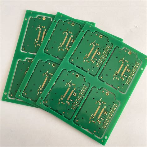
Pcb test
Importance Of PCB Testing In Electronics Manufacturing
Printed Circuit Board (PCB) testing is a critical component in the electronics manufacturing process, ensuring the reliability and functionality of electronic devices. As the backbone of modern electronic systems, PCBs serve as the foundation upon which all electronic components are mounted and interconnected. Consequently, the importance of rigorous PCB testing cannot be overstated, as it directly impacts the performance, safety, and longevity of the final product.
To begin with, PCB testing is essential for identifying manufacturing defects that could compromise the integrity of the electronic device.
These defects can range from short circuits and open circuits to misaligned components and soldering issues. By detecting such anomalies early in the production process, manufacturers can address and rectify them before the product reaches the market. This proactive approach not only enhances the quality of the final product but also reduces the likelihood of costly recalls and repairs, thereby safeguarding the manufacturer’s reputation.
Moreover, PCB testing plays a pivotal role in ensuring compliance with industry standards and regulations.
Various regulatory bodies, such as the International Electrotechnical Commission (IEC) and the Institute of Electrical and Electronics Engineers (IEEE), have established stringent guidelines for electronic devices. Adhering to these standards is crucial for manufacturers to gain market approval and avoid legal repercussions. Through comprehensive testing, manufacturers can verify that their PCBs meet these regulatory requirements, thereby facilitating smoother market entry and fostering consumer trust.
In addition to regulatory compliance, PCB testing is instrumental in optimizing the performance and reliability of electronic devices.
By subjecting PCBs to a battery of tests, including functional testing, in-circuit testing, and environmental stress testing, manufacturers can assess the board’s ability to perform under various conditions. This thorough evaluation helps identify potential weaknesses and areas for improvement, enabling manufacturers to enhance the design and robustness of their products. As a result, end-users benefit from electronic devices that are not only efficient but also durable and dependable.
Furthermore, PCB testing contributes to cost efficiency in the manufacturing process.
While the initial investment in testing equipment and procedures may seem substantial, the long-term benefits far outweigh the costs. By detecting and addressing defects early, manufacturers can minimize the incidence of product failures and returns, which can be significantly more expensive to manage. Additionally, reliable PCB testing can streamline the production process by reducing the need for rework and ensuring a higher yield of functional boards. This efficiency translates to lower production costs and improved profitability for manufacturers.
Another critical aspect of PCB testing is its role in fostering innovation within the electronics industry.
As technology continues to evolve at a rapid pace, the complexity of electronic devices increases correspondingly. Advanced PCB testing techniques, such as automated optical inspection (AOI) and X-ray inspection, enable manufacturers to keep pace with these advancements by providing precise and detailed analysis of intricate board designs. This capability not only supports the development of cutting-edge technologies but also encourages continuous improvement and innovation in PCB manufacturing processes.
In conclusion, the importance of PCB testing in electronics manufacturing cannot be overstated. It is a fundamental practice that ensures the quality, compliance, performance, and cost-efficiency of electronic devices. By investing in robust PCB testing procedures, manufacturers can deliver reliable and high-performing products to the market, thereby enhancing their competitive edge and fostering consumer confidence. As the electronics industry continues to advance, the role of PCB testing will remain indispensable in driving innovation and maintaining the highest standards of excellence.
Common Methods For PCB Testing And Their Benefits
Printed Circuit Boards (PCBs) are integral components in modern electronic devices, and ensuring their functionality and reliability is paramount. Various methods are employed to test PCBs, each offering distinct advantages. Understanding these methods and their benefits is crucial for manufacturers aiming to maintain high standards of quality and performance.
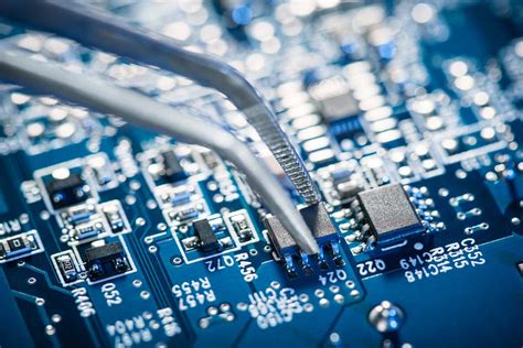
One of the most prevalent methods for PCB testing is the In-Circuit Test (ICT).
This technique involves using a bed of nails fixture to make contact with various test points on the PCB. ICT is highly effective in identifying manufacturing defects such as shorts, opens, and component failures. The primary benefit of ICT is its ability to provide comprehensive coverage, ensuring that each component on the PCB is functioning correctly. Additionally, ICT can be automated, which significantly reduces testing time and increases throughput, making it ideal for high-volume production environments.
Another widely used method is the Functional Test (FT).
Unlike ICT, which focuses on individual components, FT evaluates the PCB as a whole, ensuring that it performs its intended function within the system. This method involves applying power to the PCB and simulating its operational environment to verify its performance. The main advantage of FT is its ability to detect system-level issues that may not be apparent during ICT. By simulating real-world conditions, FT provides a more holistic assessment of the PCB’s reliability and functionality.
Complementing ICT and FT is the Flying Probe Test (FPT).
This method uses movable probes to test the electrical performance of the PCB without the need for a custom fixture. FPT is particularly beneficial for low to medium-volume production runs, where the cost of creating a custom fixture for ICT may not be justified. The flexibility of FPT allows for quick setup and adaptation to different PCB designs, making it an excellent choice for prototype testing and small batch production. Moreover, FPT can access test points that are difficult to reach with traditional ICT fixtures, providing a more thorough examination of the PCB.
In addition to these methods, Automated Optical Inspection (AOI) is a non-contact testing technique that uses cameras to visually inspect the PCB for defects.
AOI is highly effective in detecting issues such as solder joint defects, component misalignment, and missing components. The primary benefit of AOI is its speed and accuracy, as it can quickly scan the entire PCB and identify defects with high precision. This method is particularly useful in the early stages of production, allowing manufacturers to catch and rectify defects before they progress further down the production line.
Lastly, X-ray Inspection is another valuable method for PCB testing, especially for detecting hidden defects that are not visible through AOI.
This technique uses X-rays to penetrate the PCB and create detailed images of its internal structure. X-ray Inspection is particularly beneficial for identifying issues such as voids in solder joints, internal cracks, and misaligned layers. The ability to see through the PCB and examine its internal components provides a level of insight that is unmatched by other testing methods.
In conclusion, the various methods for PCB testing each offer unique benefits that contribute to the overall quality and reliability of electronic devices. In-Circuit Test, Functional Test, Flying Probe Test, Automated Optical Inspection, and X-ray Inspection all play crucial roles in identifying and rectifying defects at different stages of production. By employing a combination of these methods, manufacturers can ensure that their PCBs meet the highest standards of performance and reliability, ultimately leading to more robust and dependable electronic products.
How To Choose The Right PCB Testing Equipment
Selecting the appropriate PCB testing equipment is a critical step in ensuring the reliability and functionality of printed circuit boards (PCBs). The process involves a thorough understanding of the various testing methods available, the specific requirements of the PCB being tested, and the overall goals of the testing process. To begin with, it is essential to recognize the different types of PCB testing equipment and their respective applications. Common testing methods include in-circuit testing (ICT), functional testing, boundary scan testing, and automated optical inspection (AOI). Each of these methods serves a unique purpose and offers distinct advantages, making it imperative to match the testing equipment to the specific needs of the PCB.
In-circuit testing (ICT) is widely used for its ability to detect manufacturing defects and component failures.
This method involves using a bed of nails tester to make electrical contact with various points on the PCB, allowing for the measurement of resistance, capacitance, and other electrical parameters. ICT is particularly effective for identifying issues such as short circuits, open circuits, and incorrect component values. However, it is important to note that ICT requires a custom fixture for each PCB design, which can be costly and time-consuming to produce.
Functional testing, on the other hand, evaluates the overall performance of the PCB by simulating its operating environment.
This method involves applying power to the PCB and running a series of tests to ensure that it functions as intended. Functional testing is highly effective for verifying the performance of complex PCBs with multiple components and intricate circuitry. It is also useful for identifying issues that may not be detected by ICT, such as software-related problems or interactions between components. However, functional testing can be more time-consuming and may require specialized equipment and expertise.
Boundary scan testing, also known as JTAG testing, is a powerful method for testing PCBs with high-density interconnects and limited physical access.
This method uses a standardized interface to test the connections between components and detect faults such as open circuits and short circuits. Boundary scan testing is particularly useful for testing complex PCBs with multiple layers and fine-pitch components. It also allows for testing of individual components without the need for physical probes, making it an efficient and cost-effective solution for many applications.
Automated optical inspection (AOI) is another valuable tool for PCB testing, particularly for detecting visual defects such as solder joint issues, component misalignment, and missing components.
AOI systems use high-resolution cameras and advanced image processing algorithms to inspect PCBs at various stages of the manufacturing process. This method is highly effective for identifying defects that may not be detected by electrical testing methods, and it can be used to inspect both assembled and unassembled PCBs. However, AOI is limited to detecting visual defects and cannot evaluate the electrical performance of the PCB.
When choosing the right PCB testing equipment, it is important to consider factors such as the complexity of the PCB, the types of defects that need to be detected, and the available budget and resources. Additionally, it is essential to evaluate the capabilities and limitations of each testing method and select the equipment that best meets the specific requirements of the PCB. By carefully considering these factors and selecting the appropriate testing equipment, manufacturers can ensure the reliability and functionality of their PCBs, ultimately leading to higher quality products and increased customer satisfaction.
Troubleshooting Tips For PCB Test Failures
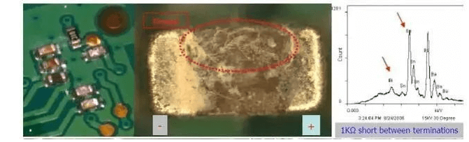
When dealing with PCB test failures, it is crucial to adopt a systematic approach to troubleshooting in order to identify and rectify the underlying issues effectively. The first step in this process involves a thorough visual inspection of the PCB. This can often reveal obvious defects such as solder bridges, missing components, or physical damage to the board. Utilizing magnification tools can enhance the ability to detect these issues, which might be missed by the naked eye.
Following the visual inspection, it is advisable to perform a continuity test.
This helps in identifying open circuits or short circuits within the PCB. Using a multimeter, one can check the connections between various points on the board to ensure that the electrical pathways are intact. If a continuity issue is detected, it is essential to trace the circuit to locate the exact point of failure.
In addition to continuity testing, it is important to verify the integrity of the power supply.
Ensuring that the correct voltage levels are present at various points on the PCB is critical. Anomalies in voltage levels can indicate issues such as faulty components or incorrect power supply connections. Using an oscilloscope can provide a more detailed view of the power signals, allowing for the detection of transient issues that might not be apparent with a simple multimeter.
Component testing is another vital aspect of troubleshooting PCB test failures.
Each component on the board should be tested individually to confirm its functionality. This includes checking resistors, capacitors, diodes, and integrated circuits. For instance, resistors can be tested for their resistance values using a multimeter, while capacitors can be checked for their capacitance and potential leakage. Integrated circuits may require more specialized testing equipment to verify their operation.
Signal integrity issues can also lead to PCB test failures.
These issues often arise from improper layout design, such as inadequate trace spacing or poor grounding practices. Using signal integrity analysis tools can help in identifying problems related to signal reflection, crosstalk, or electromagnetic interference. Addressing these issues may involve redesigning the PCB layout to ensure proper signal routing and grounding.
Another common cause of PCB test failures is thermal stress.
Excessive heat during soldering or operation can damage components or cause solder joints to fail. It is important to ensure that the soldering process is performed within the recommended temperature ranges and that adequate cooling mechanisms are in place for the PCB during operation. Thermal imaging cameras can be used to detect hotspots on the board, which can indicate areas of concern.
Software-related issues should not be overlooked when troubleshooting PCB test failures.
Firmware or software bugs can lead to unexpected behavior in the PCB. Ensuring that the latest firmware updates are applied and that the software is thoroughly tested can help in mitigating these issues. Debugging tools and techniques, such as in-circuit emulators or logic analyzers, can be invaluable in diagnosing software-related problems.
In conclusion, troubleshooting PCB test failures requires a comprehensive approach that encompasses visual inspection, electrical testing, component verification, signal integrity analysis, thermal management, and software debugging. By systematically addressing each of these areas, one can effectively identify and resolve the issues leading to test failures, thereby ensuring the reliability and functionality of the PCB.