Pcb tips and tricks
1. Plan your layout carefully: Before starting your PCB design, plan your layout carefully. Decide the placement of components, the size of the board, and the routing of traces.
2. Use a ground plane: A ground plane is a large area of copper that is connected to ground. It helps to reduce noise and interference in the circuit.
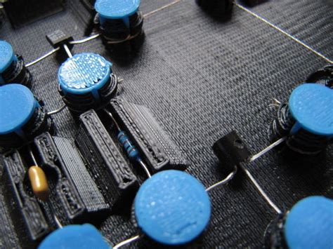
3. Keep traces short: The shorter the trace, the less resistance and capacitance it will have. This will help to reduce noise and improve signal integrity.
4. Use high-quality components: Using high-quality components will ensure that your circuit functions properly and is reliable.

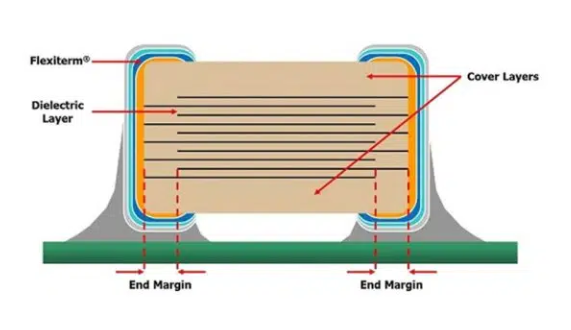
5. Use a multilayer PCB: Multilayer PCBs have more layers than single-layer PCBs,
which allows for more complex circuits. They also help to reduce noise and interference.
6. Use copper pour: Copper pour is a technique where you fill unused areas of the PCB with copper.
This helps to reduce noise and improve signal integrity.
7. Use a design rule checker: A design rule checker will check your design for errors and ensure that it meets industry standards.
8. Test your PCB: Before finalizing your design, test your PCB to ensure that it functions properly.
9. Use a good PCB software: Using a good PCB software will make the design process easier and more efficient.
10. Follow industry standards:
Follow industry standards for PCB design to ensure that your PCB is reliable and meets the required specifications.

Where to Use PCB Tips and Tricks
1. Designing PCB layouts: PCB tips and tricks can be used to design efficient and effective PCB layouts.
This includes optimizing the placement of components, routing traces, and minimizing noise and interference.
2. Troubleshooting PCBs: PCB tips and tricks can be used to diagnose and solve problems with faulty PCBs.
This includes identifying faulty components, tracing signals, and repairing damaged traces.
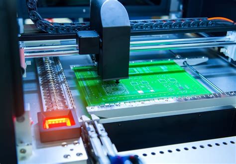
3. Manufacturing PCBs: PCB tips and tricks can be used to optimize the manufacturing process for PCBs.
This includes selecting the right materials, designing for manufacturability, and minimizing errors and defects.

4. Testing PCBs: PCB tips and tricks can be used to test and validate the functionality of PCBs.
This includes using test equipment, developing test procedures, and analyzing test results.
5. Upgrading and modifying PCBs: PCB tips and tricks can be used to upgrade and modify existing PCBs.
This includes adding new components, changing the layout, and improving performance.