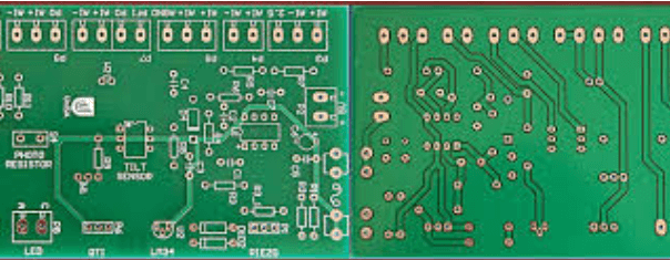
Pcb top layer
Designing Efficient PCB Top Layers for High-Speed Circuits
Designing efficient PCB top layers for high-speed circuits is a critical aspect of modern electronics engineering. As the demand for faster and more reliable electronic devices continues to grow, the need for meticulous planning and execution in PCB design becomes increasingly paramount.
The top layer of a printed circuit board (PCB) plays a crucial role in determining the overall performance and reliability of high-speed circuits.
Therefore, understanding the key considerations and best practices for designing this layer is essential for engineers and designers.
To begin with, the layout of the top layer must be carefully planned to minimize signal interference and ensure optimal signal integrity.
High-speed circuits are particularly susceptible to issues such as crosstalk, electromagnetic interference (EMI), and signal reflection. These problems can degrade the performance of the circuit and lead to data corruption or loss. To mitigate these risks, designers should prioritize the placement of critical components and signal traces on the top layer. By doing so, they can reduce the length of signal paths and minimize the potential for interference.
Moreover, the use of ground planes is a fundamental strategy in high-speed PCB design.
A continuous ground plane on the top layer can provide a low-impedance return path for high-frequency signals, thereby reducing EMI and improving signal integrity. It is advisable to place the ground plane as close to the signal traces as possible, which can be achieved by using a multilayer PCB design. This approach not only enhances the performance of high-speed circuits but also simplifies the routing process.
In addition to ground planes, the selection of materials for the top layer is another critical factor.
High-speed circuits often require materials with low dielectric constants and low loss tangents to ensure minimal signal degradation. Common materials used for high-speed PCBs include FR-4, Rogers, and Teflon. Each of these materials has its own set of properties and trade-offs, so designers must carefully evaluate their specific requirements and choose the most suitable material for their application.
Furthermore, the routing of signal traces on the top layer should be done with precision and care.
It is essential to maintain consistent trace widths and spacing to avoid impedance mismatches, which can lead to signal reflection and loss. Differential pairs, commonly used in high-speed circuits, should be routed with equal lengths and minimal separation to ensure proper signal timing and integrity. Additionally, designers should avoid sharp bends and vias in signal traces, as these can introduce discontinuities and degrade signal quality.
Thermal management is another important consideration in the design of PCB top layers for high-speed circuits.
High-speed components often generate significant amounts of heat, which can affect the performance and reliability of the circuit. To address this issue, designers can incorporate thermal vias, heat sinks, and copper pours on the top layer to dissipate heat effectively. Proper thermal management not only enhances the longevity of the components but also ensures stable operation under varying environmental conditions.
In conclusion, designing efficient PCB top layers for high-speed circuits requires a comprehensive understanding of various factors, including signal integrity, material selection, routing techniques, and thermal management. By carefully considering these aspects and implementing best practices, designers can create high-performance PCBs that meet the demands of modern electronic devices. As technology continues to advance, the importance of meticulous PCB design will only grow, making it essential for engineers to stay informed and adept in this ever-evolving field.
Common Mistakes to Avoid in PCB Top Layer Layout
When designing the top layer of a printed circuit board (PCB), it is crucial to avoid common mistakes that can compromise the functionality and reliability of the final product. One of the most frequent errors is improper component placement. Placing components too close to each other can lead to difficulties in soldering and increased risk of short circuits. To mitigate this, it is essential to follow the manufacturer’s recommended spacing guidelines and ensure that there is adequate room for soldering and inspection.
Another common mistake is neglecting thermal management.
Components that generate significant heat, such as power transistors and voltage regulators, should be strategically placed to allow for efficient heat dissipation. Failing to do so can result in overheating, which can degrade the performance and lifespan of the components. Utilizing thermal vias and heat sinks can help manage heat more effectively, ensuring the PCB operates within safe temperature limits.
Signal integrity is another critical aspect that can be compromised by poor layout practices.
High-speed signals should be routed with care to minimize noise and signal degradation. One common error is not maintaining consistent trace impedance, which can lead to signal reflections and data corruption. To avoid this, designers should use controlled impedance traces and maintain consistent trace widths and spacing. Additionally, keeping high-speed signal traces as short as possible and avoiding sharp bends can further enhance signal integrity.
Grounding issues are also a prevalent problem in PCB top layer design.
A poor grounding strategy can lead to electromagnetic interference (EMI) and signal integrity problems. To address this, designers should use a solid ground plane and ensure that all components have a low-impedance path to ground. Stitching vias can be used to connect the ground plane on the top layer to other layers, providing a more robust grounding system.
Power distribution is another area where mistakes are commonly made.
Inadequate power trace widths can lead to voltage drops and excessive heating. It is important to calculate the current requirements of each trace and ensure that they are wide enough to handle the expected current without significant voltage drop or overheating. Using power planes instead of traces can also help distribute power more evenly and reduce the risk of voltage drops.
Component orientation is another factor that can impact the manufacturability and testability of the PCB.
Placing components in a consistent orientation can simplify the assembly process and reduce the likelihood of errors. It also makes it easier to inspect and test the board, as the orientation of components will be predictable.
Lastly, neglecting design for manufacturability (DFM) guidelines can lead to production issues and increased costs.
DFM guidelines are designed to ensure that the PCB can be manufactured efficiently and reliably. Ignoring these guidelines can result in boards that are difficult or impossible to produce, leading to delays and increased costs. It is important to work closely with the PCB manufacturer to ensure that the design meets their capabilities and requirements.
In conclusion, avoiding common mistakes in PCB top layer layout requires careful consideration of component placement, thermal management, signal integrity, grounding, power distribution, component orientation, and manufacturability. By paying attention to these factors and following best practices, designers can create PCBs that are reliable, efficient, and cost-effective.

Optimizing Signal Integrity on the PCB Top Layer
Optimizing signal integrity on the PCB top layer is a critical aspect of modern electronic design, ensuring that signals are transmitted with minimal distortion and interference. The top layer of a printed circuit board (PCB) often serves as the primary routing layer for high-speed signals, making its design paramount to the overall performance of the electronic device. To achieve optimal signal integrity, several key considerations must be taken into account, including trace layout, impedance control, and the minimization of electromagnetic interference (EMI).
Firstly, the layout of traces on the PCB top layer plays a significant role in maintaining signal integrity.
Traces should be kept as short and direct as possible to reduce the potential for signal degradation. Additionally, it is essential to maintain consistent trace widths and spacing to ensure uniform impedance, which is crucial for high-speed signal transmission. When routing differential pairs, such as those used in high-speed data interfaces, it is important to keep the traces closely coupled and of equal length to prevent skew and maintain signal integrity.
Moreover, impedance control is a fundamental aspect of optimizing signal integrity on the PCB top layer.
Impedance mismatches can lead to signal reflections, which can cause data errors and degrade overall system performance. To achieve controlled impedance, designers must carefully select the trace width, spacing, and the dielectric material of the PCB. Utilizing simulation tools during the design phase can help predict and adjust the impedance of traces, ensuring that they meet the required specifications.
In addition to trace layout and impedance control, minimizing electromagnetic interference (EMI) is crucial for maintaining signal integrity on the PCB top layer.
EMI can originate from various sources, including other components on the PCB, external devices, and even the traces themselves. To mitigate EMI, designers should implement proper grounding techniques, such as using a solid ground plane on an adjacent layer to the top layer. This ground plane provides a return path for signals, reducing the potential for EMI and improving signal integrity.
Furthermore, the placement of components on the PCB top layer can significantly impact signal integrity.
High-speed components should be placed as close to their corresponding connectors or interfaces as possible to minimize trace lengths and reduce the potential for signal degradation. Additionally, sensitive analog components should be isolated from high-speed digital traces to prevent interference and crosstalk.
Another important consideration is the use of decoupling capacitors to stabilize power delivery and reduce noise on the PCB top layer.
Placing decoupling capacitors close to the power pins of integrated circuits can help filter out high-frequency noise and provide a stable power supply, which is essential for maintaining signal integrity.
Finally, it is important to conduct thorough testing and validation of the PCB design to ensure optimal signal integrity.
This includes performing signal integrity simulations, conducting impedance measurements, and using tools such as time-domain reflectometry (TDR) to identify and address any potential issues. By rigorously testing the PCB design, designers can identify and mitigate any factors that may compromise signal integrity, ensuring reliable and high-performance operation of the electronic device.
In conclusion, optimizing signal integrity on the PCB top layer requires careful consideration of trace layout, impedance control, EMI minimization, component placement, and power delivery. By addressing these factors during the design phase and conducting thorough testing, designers can ensure that their PCBs deliver reliable and high-performance signal transmission, meeting the demands of modern electronic applications.
Thermal Management Techniques for PCB Top Layers
Effective thermal management is crucial for the optimal performance and longevity of printed circuit boards (PCBs), particularly in high-power applications. The top layer of a PCB plays a significant role in dissipating heat, and various techniques can be employed to enhance its thermal management capabilities. Understanding these techniques is essential for engineers and designers aiming to improve the reliability and efficiency of electronic devices.
One fundamental approach to thermal management on the PCB top layer is the use of thermal vias.
These are small, plated holes that connect the top layer to internal or bottom layers, facilitating the transfer of heat away from critical components. By strategically placing thermal vias beneath heat-generating components, designers can create a more efficient heat dissipation path. This method is particularly effective when combined with a ground plane or a dedicated thermal plane on an internal layer, which can further spread the heat across a larger area.
In addition to thermal vias, the use of copper pours or planes on the top layer can significantly enhance thermal performance.
Copper has excellent thermal conductivity, and by increasing the copper area around heat-generating components, the heat can be spread more evenly and dissipated more effectively. This technique is often used in conjunction with thermal vias to create a comprehensive thermal management system. Moreover, thicker copper layers can be employed to further improve heat dissipation, although this may increase the cost and complexity of the PCB manufacturing process.
Another technique involves the use of thermal pads or heat sinks directly on the top layer.
Thermal pads are typically made of materials with high thermal conductivity and are placed between the component and the PCB to facilitate heat transfer. Heat sinks, on the other hand, are external components that attach to the PCB and provide additional surface area for heat dissipation. Both methods can be highly effective, especially when dealing with components that generate substantial amounts of heat, such as power transistors or processors.
Furthermore, the layout and placement of components on the top layer can significantly impact thermal management.
By positioning high-power components away from each other and from temperature-sensitive components, designers can minimize localized hotspots and ensure more uniform heat distribution. Additionally, aligning components along the airflow path in systems with active cooling can enhance the efficiency of heat removal.
The choice of materials for the PCB substrate also plays a critical role in thermal management.
High thermal conductivity materials, such as metal-core PCBs or ceramics, can provide superior heat dissipation compared to traditional FR4 substrates. While these materials may come at a higher cost, their thermal performance benefits can be invaluable in high-power applications.
Lastly, thermal simulation and analysis tools are indispensable in the design process.
These tools allow engineers to model the thermal behavior of the PCB and identify potential issues before physical prototypes are built. By simulating different thermal management techniques and configurations, designers can optimize the PCB layout for maximum thermal efficiency.
In conclusion, effective thermal management on the PCB top layer is achieved through a combination of techniques, including the use of thermal vias, copper pours, thermal pads, heat sinks, strategic component placement, and advanced materials. By carefully considering these factors and utilizing thermal simulation tools, designers can enhance the thermal performance of their PCBs, ensuring the reliability and longevity of electronic devices.