Pcb trace width rf
Importance Of PCB Trace Width RF Design
In the realm of radio frequency (RF) design, the importance of printed circuit board (PCB) trace width cannot be overstated. The trace width on a PCB plays a critical role in determining the performance, reliability, and efficiency of RF circuits.
As RF signals operate at high frequencies, typically ranging from 3 kHz to 300 GHz, the design considerations for PCB traces become significantly more complex compared to low-frequency circuits. Understanding the implications of trace width in RF design is essential for engineers aiming to optimize signal integrity and minimize losses.
One of the primary reasons trace width is crucial in RF design is its direct impact on impedance control.
Impedance, which is the measure of opposition that a circuit presents to the flow of alternating current, must be carefully managed to ensure signal integrity. In RF circuits, maintaining a consistent impedance is vital to prevent signal reflections, which can lead to signal degradation and loss. The trace width, along with the dielectric material and the distance between the trace and the ground plane, determines the characteristic impedance of the trace. Therefore, precise control over trace width is necessary to match the impedance of the trace with the source and load, thereby minimizing reflections and ensuring efficient signal transmission.
Moreover, the trace width influences the resistance and inductance of the PCB traces, which are critical parameters in RF design.
Narrow traces exhibit higher resistance, which can lead to increased signal attenuation and power loss. This is particularly problematic in high-frequency applications where even small losses can significantly impact performance. Conversely, wider traces reduce resistance but may introduce unwanted parasitic capacitance, which can affect the signal’s phase and amplitude. Therefore, finding an optimal trace width that balances resistance and capacitance is essential for maintaining signal integrity and achieving the desired performance in RF circuits.
In addition to impedance control and resistance considerations, the trace width also affects thermal management in RF designs.
High-frequency signals can generate significant amounts of heat, and narrow traces may not be able to dissipate this heat effectively. This can lead to overheating and potential damage to the PCB and its components. Wider traces, on the other hand, provide better thermal conductivity, allowing for more efficient heat dissipation. This is particularly important in high-power RF applications where thermal management is a critical concern. By optimizing the trace width, engineers can ensure that the PCB operates within safe temperature limits, thereby enhancing the reliability and longevity of the RF circuit.
Furthermore, the manufacturing process and tolerances must be considered when determining the appropriate trace width for RF designs.
Variations in the etching process can lead to deviations in the actual trace width from the intended design, which can impact the impedance and overall performance of the circuit. Therefore, it is essential to account for manufacturing tolerances and ensure that the chosen trace width can be consistently produced within acceptable limits. This requires close collaboration with PCB manufacturers and a thorough understanding of their capabilities and limitations.
In conclusion, the importance of PCB trace width in RF design cannot be underestimated. It plays a pivotal role in impedance control, resistance and inductance management, thermal dissipation, and manufacturability. By carefully considering and optimizing trace width, engineers can enhance signal integrity, minimize losses, and ensure the reliable operation of RF circuits. As RF technology continues to advance and find applications in various fields, the meticulous design of PCB traces will remain a cornerstone of successful RF engineering.
Calculating Optimal PCB Trace Width For RF Circuits
Calculating the optimal PCB trace width for RF circuits is a critical aspect of designing high-frequency electronic systems. The performance of RF circuits is highly sensitive to the physical characteristics of the PCB traces, which act as transmission lines. Therefore, understanding the factors that influence trace width is essential for ensuring signal integrity and minimizing losses.
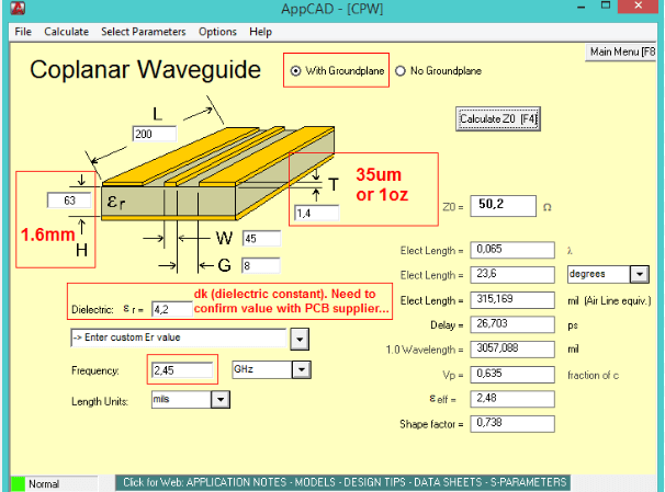
One of the primary considerations in determining the optimal trace width is the characteristic impedance of the transmission line.
The characteristic impedance is a function of the trace width, the dielectric constant of the PCB material, and the distance between the trace and the reference plane. For RF circuits, maintaining a consistent characteristic impedance is crucial to prevent signal reflections and ensure efficient power transfer. Typically, a characteristic impedance of 50 ohms is standard for most RF applications. To achieve this, designers must carefully calculate the trace width based on the specific PCB stack-up and material properties.
In addition to characteristic impedance, the skin effect plays a significant role in RF trace width calculations.
At high frequencies, the current tends to flow on the surface of the conductor, effectively reducing the cross-sectional area available for current flow. This phenomenon increases the effective resistance of the trace, leading to higher insertion losses. To mitigate the skin effect, designers often opt for wider traces or use materials with lower resistivity, such as copper with a higher purity level. However, increasing the trace width can also impact the characteristic impedance, necessitating a careful balance between these factors.
Thermal management is another critical aspect to consider when calculating PCB trace width for RF circuits.
High-frequency signals can generate significant heat due to resistive losses, which can degrade the performance and reliability of the circuit. Wider traces can help dissipate heat more effectively, reducing the risk of thermal damage. However, the PCB layout must also accommodate the physical constraints of the design, such as component placement and routing density. Therefore, designers must evaluate the thermal performance of the traces in conjunction with other design parameters.
Moreover, the choice of PCB material significantly influences the optimal trace width for RF circuits.
Materials with lower dielectric constants and loss tangents are preferred for high-frequency applications, as they minimize signal attenuation and dispersion. Common materials include FR-4, Rogers, and Teflon-based laminates. Each material has unique properties that affect the trace width calculation, and designers must select the appropriate material based on the specific requirements of the RF circuit.
Furthermore, manufacturing tolerances and variations in the PCB fabrication process can impact the final trace width.
Factors such as etching precision, layer alignment, and copper thickness can introduce deviations from the intended design. To account for these variations, designers often include a margin of error in their calculations, ensuring that the final product meets the desired performance specifications.
In conclusion, calculating the optimal PCB trace width for RF circuits involves a comprehensive analysis of multiple factors, including characteristic impedance, skin effect, thermal management, material properties, and manufacturing tolerances. By carefully considering these elements, designers can achieve a balance that ensures signal integrity, minimizes losses, and enhances the overall performance of the RF circuit. This meticulous approach is essential for the successful design and implementation of high-frequency electronic systems.
Common Mistakes In PCB Trace Width For RF Applications
Designing printed circuit boards (PCBs) for radio frequency (RF) applications requires meticulous attention to detail, particularly when it comes to trace width. One common mistake in PCB trace width for RF applications is underestimating the importance of impedance control. RF signals are highly sensitive to impedance mismatches, which can lead to signal reflections, loss, and overall degradation of performance. Designers often overlook the need to calculate the correct trace width to maintain a consistent impedance, which is crucial for ensuring signal integrity.
Another frequent error is neglecting the impact of the PCB substrate material on trace width.
Different materials have varying dielectric constants, which affect the impedance of the traces. Failing to account for these variations can result in improper trace widths, leading to impedance mismatches. It is essential to select a substrate material with a known dielectric constant and use it in the calculations for determining the appropriate trace width.
Additionally, designers sometimes ignore the effect of trace thickness on impedance.
The thickness of the copper traces can influence the overall impedance, and failing to consider this factor can lead to inaccuracies in the trace width calculations. It is important to use the correct copper thickness in the design process to ensure that the impedance remains consistent across the PCB.
Moreover, inadequate spacing between traces is another common mistake. In RF applications, traces that are too close together can cause crosstalk and electromagnetic interference (EMI), which can severely impact the performance of the circuit. Ensuring adequate spacing between traces is crucial to minimize these issues and maintain signal integrity.
Furthermore, designers often overlook the importance of proper grounding in RF PCB design.
A poor grounding strategy can lead to increased noise and signal degradation. It is essential to implement a solid ground plane and ensure that the traces are properly referenced to this ground plane to minimize noise and maintain signal integrity.
Another mistake is failing to consider the impact of vias on trace impedance.
Vias can introduce inductance and capacitance, which can affect the impedance of the traces. It is important to minimize the use of vias in critical RF signal paths and, when necessary, use techniques such as back-drilling to reduce their impact on impedance.
Additionally, designers sometimes neglect the importance of thermal management in RF PCB design.
High-frequency signals can generate significant heat, which can affect the performance and reliability of the circuit. Ensuring proper thermal management, such as using thermal vias and heat sinks, is crucial to maintaining the performance and longevity of the RF circuit.
Lastly, inadequate testing and validation of the PCB design can lead to issues in RF applications.
It is essential to thoroughly test and validate the PCB design to ensure that the trace widths and other design parameters meet the required specifications. This includes using tools such as time-domain reflectometry (TDR) and vector network analyzers (VNA) to measure and verify the impedance and signal integrity of the traces.
In conclusion, designing PCB trace widths for RF applications requires careful consideration of various factors, including impedance control, substrate material, trace thickness, spacing, grounding, vias, thermal management, and thorough testing. By avoiding these common mistakes, designers can ensure that their RF circuits perform optimally and maintain signal integrity.
Advanced Techniques For Managing PCB Trace Width In RF Systems
In the realm of radio frequency (RF) systems, managing PCB trace width is a critical aspect that demands meticulous attention. The performance of RF circuits is highly sensitive to the physical characteristics of the PCB traces, which serve as the conduits for high-frequency signals. Therefore, understanding and implementing advanced techniques for managing PCB trace width is essential for ensuring optimal functionality and reliability of RF systems.
One of the primary considerations in managing PCB trace width in RF systems is impedance control.
Impedance mismatches can lead to signal reflections, which degrade the signal integrity and overall performance of the RF circuit. To achieve the desired impedance, designers must carefully calculate the trace width, taking into account the dielectric constant of the PCB material, the height of the trace above the ground plane, and the trace thickness. Utilizing tools such as impedance calculators and simulation software can aid in determining the precise trace width required to maintain consistent impedance throughout the circuit.
In addition to impedance control, minimizing signal loss is another crucial factor.
Signal loss, or attenuation, can occur due to the resistive properties of the trace material and the dielectric losses in the PCB substrate. To mitigate these losses, designers often opt for materials with lower loss tangents and employ wider traces to reduce resistive losses. However, wider traces can also introduce parasitic capacitance, which can adversely affect the performance of high-frequency signals. Therefore, a balanced approach is necessary, where the trace width is optimized to minimize both resistive and dielectric losses while maintaining the desired impedance.
Moreover, managing PCB trace width in RF systems also involves addressing issues related to crosstalk and electromagnetic interference (EMI).
Crosstalk occurs when signals from adjacent traces couple into each other, leading to unwanted interference and signal degradation. To minimize crosstalk, designers can increase the spacing between traces, use ground planes to provide shielding, and implement differential signaling techniques. Additionally, careful routing of traces and the use of guard traces can further reduce the potential for crosstalk and EMI.
Thermal management is another aspect that cannot be overlooked when dealing with PCB trace width in RF systems.
High-frequency signals can generate significant heat, which can affect the performance and longevity of the PCB. Wider traces can help dissipate heat more effectively, but this must be balanced with the need to maintain the desired impedance and minimize signal loss. Employing thermal vias and heat sinks can also aid in managing the thermal load on the PCB.
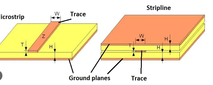
Furthermore, advanced techniques such as the use of microstrip and stripline configurations can enhance the performance of RF circuits.
Microstrip lines, which consist of a trace on the surface of the PCB with a ground plane beneath, are commonly used for their simplicity and ease of manufacturing. Striplines, on the other hand, are embedded between two ground planes, providing better shielding and reduced radiation losses. The choice between microstrip and stripline configurations depends on the specific requirements of the RF system, including the operating frequency, signal integrity, and manufacturing constraints.
In conclusion, managing PCB trace width in RF systems is a multifaceted challenge that requires a comprehensive understanding of various factors, including impedance control, signal loss, crosstalk, EMI, and thermal management. By employing advanced techniques and leveraging simulation tools, designers can optimize trace width to ensure the efficient and reliable performance of RF circuits. As RF technology continues to evolve, staying abreast of the latest advancements and best practices in PCB design will be crucial for achieving success in this dynamic field.
Importance Of PCB Trace Width In RF Design
In the realm of radio frequency (RF) design, the importance of printed circuit board (PCB) trace width cannot be overstated. The trace width on a PCB plays a critical role in determining the performance, reliability, and efficiency of RF circuits. As RF signals operate at high frequencies, typically ranging from 3 kHz to 300 GHz, the design considerations for PCB traces become significantly more complex compared to low-frequency circuits. Understanding the implications of trace width in RF design is essential for engineers aiming to optimize signal integrity and minimize losses.
One of the primary reasons trace width is crucial in RF design is its direct impact on impedance control.
Impedance, which is the measure of opposition that a circuit presents to the flow of alternating current, must be carefully managed to ensure signal integrity. In RF circuits, maintaining a consistent impedance is vital to prevent signal reflections, which can lead to signal degradation and loss. The trace width, along with the dielectric material and the distance between the trace and the ground plane, determines the characteristic impedance of the trace. Therefore, precise control over trace width is necessary to match the impedance of the trace with the source and load, thereby minimizing reflections and ensuring efficient signal transmission.
Moreover, the trace width influences the resistance and inductance of the PCB traces, which are critical parameters in RF design.
Narrow traces exhibit higher resistance, which can lead to increased signal attenuation and power loss. This is particularly problematic in high-frequency applications where even small losses can significantly impact performance. Conversely, wider traces reduce resistance but may introduce unwanted parasitic capacitance, which can affect the signal’s phase and amplitude. Therefore, finding an optimal trace width that balances resistance and capacitance is essential for maintaining signal integrity and achieving the desired performance in RF circuits.
In addition to impedance control and resistance considerations, the trace width also affects thermal management in RF designs.
High-frequency signals can generate significant amounts of heat, and narrow traces may not be able to dissipate this heat effectively. This can lead to overheating and potential damage to the PCB and its components. Wider traces, on the other hand, provide better thermal conductivity, allowing for more efficient heat dissipation. This is particularly important in high-power RF applications where thermal management is a critical concern. By optimizing the trace width, engineers can ensure that the PCB operates within safe temperature limits, thereby enhancing the reliability and longevity of the RF circuit.
Furthermore, the manufacturing process and tolerances must be considered when determining the appropriate trace width for RF designs.
Variations in the etching process can lead to deviations in the actual trace width from the intended design, which can impact the impedance and overall performance of the circuit. Therefore, it is essential to account for manufacturing tolerances and ensure that the chosen trace width can be consistently produced within acceptable limits. This requires close collaboration with PCB manufacturers and a thorough understanding of their capabilities and limitations.
In conclusion, the importance of PCB trace width in RF design cannot be underestimated. It plays a pivotal role in impedance control, resistance and inductance management, thermal dissipation, and manufacturability. By carefully considering and optimizing trace width, engineers can enhance signal integrity, minimize losses, and ensure the reliable operation of RF circuits. As RF technology continues to advance and find applications in various fields, the meticulous design of PCB traces will remain a cornerstone of successful RF engineering.