PCB Transmission Line Principles: A Comprehensive Guide
Introduction to PCB Transmission Lines
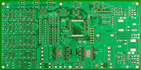
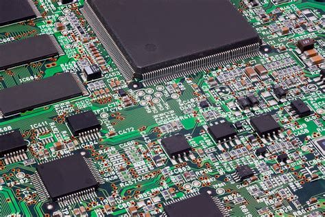
In modern high-speed digital and high-frequency analog circuits, printed circuit board (PCB) transmission lines play a critical role in maintaining signal integrity. As clock frequencies continue to increase and rise times become faster, what were once simple conductive traces must now be treated as transmission lines with complex electromagnetic behavior.
A PCB transmission line is a conductor structure designed to carry electrical signals from one point to another while maintaining controlled impedance and minimizing signal distortion. Unlike low-frequency circuits where wires are considered perfect conductors with negligible delay, transmission line theory becomes essential when the signal’s rise time is shorter than the round-trip propagation delay along the line.
Fundamental Concepts of Transmission Lines
Transmission Line Theory Basics
At high frequencies, PCB traces exhibit distributed impedance characteristics rather than simple resistance. This means we must consider them as having series inductance and resistance along their length, with shunt capacitance and conductance between the conductor and its return path. These distributed parameters give rise to the concept of characteristic impedance (Z₀), which represents the ratio of voltage to current for a wave propagating along the line.
The characteristic impedance of a transmission line is given by:
Z₀ = √[(R + jωL)/(G + jωC)]
Where:
- R = series resistance per unit length
- L = series inductance per unit length
- G = shunt conductance per unit length
- C = shunt capacitance per unit length
- ω = angular frequency (2πf)
For lossless lines (which is a reasonable approximation for most PCB applications), this simplifies to:
Z₀ = √(L/C)
Propagation Velocity and Delay
Signals don’t travel instantaneously through transmission lines. The propagation velocity (v) of a signal in a transmission line is given by:
v = 1/√(LC) = c/√(εᵣ)
Where:
- c = speed of light in vacuum (≈3×10⁸ m/s)
- εᵣ = effective relative permittivity (dielectric constant) of the PCB material
The propagation delay (tₚ) per unit length is:
tₚ = √(LC) = √(εᵣ)/c
Typical FR4 PCB material has εᵣ ≈ 4.0-4.5, resulting in a propagation delay of about 140-150 ps/inch (55-60 ps/cm).
Types of PCB Transmission Lines
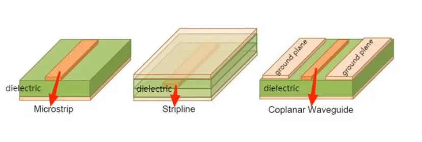
Microstrip Lines
Microstrip is the most common PCB transmission line configuration, consisting of a signal trace on the outer layer of the board with a reference plane (usually ground) on an adjacent inner layer. The characteristic impedance depends on:
- Trace width (w)
- Trace thickness (t)
- Dielectric thickness (h)
- Dielectric constant (εᵣ)
The approximate impedance of a microstrip line can be calculated using:
For w/h ≤ 1:
Z₀ = (60/√εₑff) × ln(8h/w + 0.25w/h)
For w/h ≥ 1:
Z₀ = (120π/√εₑff)/(w/h + 1.393 + 0.667ln(w/h + 1.444))
Where εₑff is the effective dielectric constant accounting for the mixed air/dielectric environment.
Stripline
Stripline consists of a signal trace sandwiched between two reference planes in the inner layers of the PCB. This symmetric structure provides better shielding and more consistent impedance than microstrip but is more challenging to route. The impedance of a stripline is given by:
Z₀ = (30π/√εᵣ) × ln(1 + 4h/(0.67πw(0.8 + t/w)))
Where:
- h = distance between planes
- w = trace width
- t = trace thickness
Coplanar Waveguide (CPW)
Coplanar waveguide features a signal trace with ground planes on the same layer on both sides. This configuration offers good high-frequency performance and easier integration with surface-mounted components. The impedance depends on:
- Central conductor width
- Gap between conductor and ground planes
- Dielectric thickness
- Dielectric constant
Transmission Line Effects in PCBs
Reflections and Impedance Matching
When a signal encounters an impedance discontinuity (such as a connector, via, or change in trace geometry), part of the signal reflects back toward the source. These reflections can cause signal integrity issues like ringing and overshoot. To minimize reflections, transmission lines must be properly terminated with matching impedances.
Common termination techniques include:
- Series termination (source termination)
- Parallel termination (end termination)
- Thevenin termination
- AC termination
Crosstalk
Crosstalk occurs when energy from one transmission line couples to adjacent lines through mutual capacitance and inductance. There are two types:
- Near-end crosstalk (NEXT)
- Far-end crosstalk (FEXT)
To minimize crosstalk:
- Increase spacing between traces
- Use guard traces with via stitching
- Route sensitive traces on different layers with orthogonal routing
- Reduce parallel run lengths between traces
Loss Mechanisms
PCB transmission lines exhibit several loss mechanisms that become significant at high frequencies:
- Conductor loss (due to finite conductivity and skin effect)
- Dielectric loss (energy absorbed by the PCB material)
- Radiation loss (energy lost as electromagnetic radiation)
The total loss is typically expressed in dB per unit length and increases with frequency.
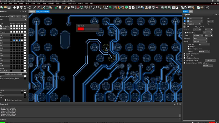
Design Considerations for PCB Transmission Lines
Impedance Control
Maintaining consistent impedance throughout the signal path is crucial for signal integrity. This requires:
- Careful calculation of trace geometries
- Consideration of manufacturing tolerances
- Accounting for discontinuities (vias, connectors, etc.)
- Using appropriate stackup designs
Routing Guidelines
Proper routing techniques help maintain signal integrity:
- Keep transmission lines as short as possible
- Avoid sharp bends (use 45° angles or curves)
- Minimize layer transitions
- Provide adequate return paths for high-speed signals
- Follow the 3W rule (spacing between traces ≥ 3× trace width)
Material Selection
The choice of PCB material significantly affects transmission line performance:
- Standard FR4 is cost-effective but has higher loss at high frequencies
- High-frequency laminates (Rogers, Isola, etc.) offer better performance but at higher cost
- Consider dielectric constant, loss tangent, and consistency
Advanced Topics in PCB Transmission Lines
Differential Transmission Lines
Differential signaling uses a pair of transmission lines carrying equal and opposite signals. This offers advantages including:
- Improved noise immunity
- Reduced electromagnetic interference (EMI)
- Tolerance to reference plane variations
Common differential pair configurations include:
- Edge-coupled microstrip
- Broadside-coupled stripline
- Edge-coupled stripline
Discontinuity Modeling
Transmission line discontinuities such as vias, bends, and connectors must be carefully modeled and compensated for:
- Via stubs can cause resonances (use back-drilling or blind vias)
- Bends require mitering or special compensation
- Connectors should have controlled impedance transitions
Signal Integrity Analysis
Modern PCB design requires sophisticated analysis tools:
- 2D field solvers for impedance calculation
- 3D EM simulators for complex structures
- Time-domain reflectometry (TDR) for verification
- Eye diagram analysis for high-speed serial links
Practical Implementation
Manufacturing Considerations
Real-world PCB fabrication introduces challenges:
- Etch factor affects final trace width and impedance
- Copper roughness impacts high-frequency loss
- Dielectric thickness variations affect impedance consistency
- Surface finishes (ENIG, immersion silver, etc.) influence performance
Measurement Techniques
Verifying transmission line performance requires proper measurement:
- Impedance measurement using TDR
- Insertion loss measurement with VNA
- Crosstalk characterization
- Time-domain measurements for digital signals
Future Trends
As data rates continue to increase, PCB transmission line technology evolves:
- Ultra-low loss materials
- Advanced via structures
- Embedded active components
- Photonic integration
- AI-assisted design optimization
Conclusion
Understanding PCB transmission line principles is essential for designing modern high-speed electronic systems. By properly applying transmission line theory, engineers can create PCBs that maintain signal integrity, minimize noise and interference, and reliably operate at increasingly higher frequencies. As technology advances, the importance of transmission line considerations in PCB design will only continue to grow.