PCB Upgrade Optimization: Strategies for Enhanced Performance and Reliability
Introduction
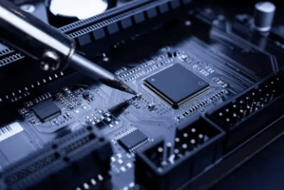
Printed Circuit Boards (PCBs) are the backbone of modern electronics, serving as the foundation for components and interconnections in devices ranging from smartphones to industrial machinery. As technology advances, optimizing PCB designs through upgrades becomes essential to improve performance, reliability, and manufacturability. This article explores key strategies for PCB upgrade optimization, covering material selection, layout improvements, signal integrity enhancements, thermal management, and manufacturing considerations.
1. Material Selection for Performance and Reliability
High-Frequency and High-Speed Materials
As electronic devices operate at higher frequencies, traditional PCB materials like FR-4 may not suffice due to signal loss and dielectric dispersion. Upgrading to advanced materials such as Rogers, Teflon, or ceramic-filled laminates can reduce signal attenuation and improve impedance control.
- Low Dielectric Constant (Dk) Materials: Reduce signal propagation delay.
- Low Loss Tangent (Df) Materials: Minimize signal loss in high-frequency applications (e.g., 5G, RF circuits).
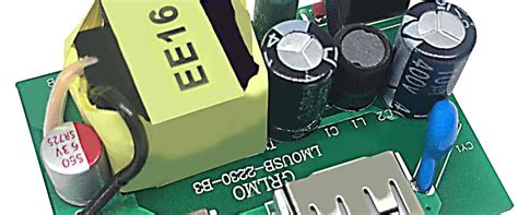
Thermal Management Materials
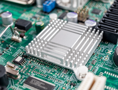
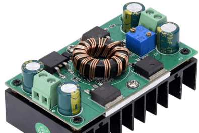
For power electronics and high-current applications, thermal performance is critical. Upgrading to metal-core PCBs (e.g., aluminum or copper substrates) or using thermally conductive dielectric layers can enhance heat dissipation.
- Metal-Core PCBs (MCPCBs): Ideal for LED lighting and power converters.
- Thermal Vias: Improve heat transfer from hot components to heat sinks.
2. Layout Optimization for Signal Integrity
Controlled Impedance Routing
High-speed digital and RF circuits require precise impedance matching to prevent reflections and signal degradation.
- Trace Width and Spacing Adjustments: Use impedance calculators to optimize for target values (e.g., 50Ω or 100Ω differential pairs).
- Stripline vs. Microstrip: Choose appropriate transmission line structures based on layer stack-up.
Crosstalk Reduction
Unwanted electromagnetic coupling between traces can degrade signal quality.
- Increased Spacing Between Critical Traces: Follow the 3W rule (trace spacing ≥ 3× trace width).
- Ground Shielding: Insert ground planes between sensitive signals.
Power Integrity Enhancements
Voltage drops and noise can disrupt circuit operation.
- Decoupling Capacitors: Place near IC power pins to suppress high-frequency noise.
- Power Plane Segmentation: Isolate noisy digital and sensitive analog power domains.
3. Thermal Management Strategies
Heat Dissipation Techniques
Overheating reduces component lifespan and reliability.
- Thermal Pads and Heat Sinks: Improve heat transfer from components.
- Copper Pouring: Increase copper area in power traces to distribute heat.
Simulation-Driven Design
Use thermal analysis tools (e.g., ANSYS, SolidWorks Flow Simulation) to predict hotspots and optimize layouts before fabrication.
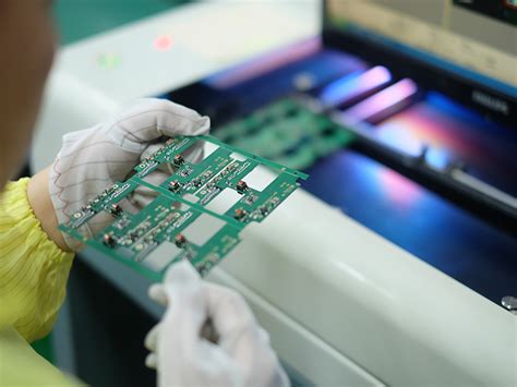
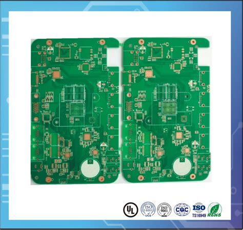
4. Manufacturing and Assembly Considerations
Design for Manufacturability (DFM)
Optimize the PCB for cost-effective and error-free production.
- Avoid Tight Tolerances: Unless necessary, relax spacing rules to reduce fabrication costs.
- Panelization: Optimize board arrays for efficient assembly.
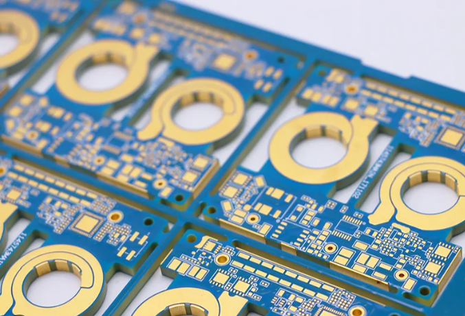
Surface Finish Upgrades
The choice of surface finish affects solderability and reliability.
- ENIG (Electroless Nickel Immersion Gold): Excellent for fine-pitch components.
- OSP (Organic Solderability Preservative): Cost-effective for consumer electronics.
5. Testing and Validation
Signal Integrity Testing
Use time-domain reflectometry (TDR) and vector network analyzers (VNA) to verify impedance and loss characteristics.
Thermal Testing
Infrared cameras and thermocouples help validate thermal performance.
Conclusion
PCB upgrade optimization is a multi-faceted process involving material selection, layout refinements, thermal management, and manufacturing improvements. By adopting these strategies, engineers can enhance performance, extend product lifespan, and reduce production costs. As electronics continue to evolve, staying ahead in PCB design optimization will be key to maintaining competitiveness in the industry.
This article provides a structured overview of PCB upgrade optimization. Let me know if you’d like to expand on any section or include specific case studies!