Pcb via current
Understanding PCB Via Current Capacity
Printed Circuit Boards (PCBs) are the backbone of modern electronic devices, providing the necessary pathways for electrical signals to travel between various components.
One critical aspect of PCB design is understanding the current capacity of vias, which are the small conductive holes that connect different layers of a PCB.
The current capacity of a via is a crucial factor in ensuring the reliability and performance of the electronic device.
To begin with, vias are essential in multi-layer PCBs, as they facilitate the vertical connection between different layers.
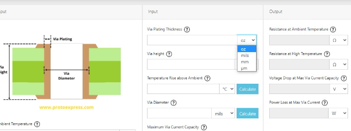
These connections are made by drilling holes through the PCB and then plating them with a conductive material, typically copper. The current-carrying capacity of a via is determined by several factors, including the via’s diameter, the thickness of the copper plating, and the thermal properties of the PCB material.
One of the primary considerations in determining via current capacity is the via’s diameter.
Larger diameter vias can carry more current because they have a greater cross-sectional area for the current to flow through. However, increasing the via diameter also takes up more space on the PCB, which can be a limiting factor in densely packed designs. Therefore, designers must strike a balance between via size and the available PCB real estate.
Another important factor is the thickness of the copper plating inside the via.
Thicker copper plating can handle higher current levels because it reduces the resistance and improves the via’s ability to dissipate heat. The standard copper thickness for PCB vias is typically 1 oz/ft², but for higher current applications, thicker copper plating, such as 2 oz/ft² or even 3 oz/ft², may be used. This increased thickness enhances the via’s current-carrying capacity and helps prevent overheating and potential failure.
Thermal management is also a critical aspect of via current capacity.
As current flows through a via, it generates heat due to the resistance of the conductive material. If this heat is not adequately dissipated, it can lead to increased temperatures, which may degrade the via’s performance and potentially damage the PCB. To mitigate this, designers often use thermal vias, which are vias specifically designed to transfer heat away from critical components and distribute it more evenly across the PCB. Additionally, the choice of PCB material can impact thermal performance, with materials that have higher thermal conductivity being more effective at dissipating heat.
Furthermore, the current capacity of a via is influenced by the overall design and layout of the PCB.
For instance, the proximity of other vias and traces can affect heat dissipation and current distribution. Designers must consider the entire PCB layout to ensure that vias are not overloaded and that heat is managed effectively. Simulation tools and software can aid in this process by allowing designers to model the thermal and electrical behavior of the PCB and optimize the via placement and size accordingly.
In conclusion, understanding the current capacity of PCB vias is essential for designing reliable and high-performance electronic devices.
By considering factors such as via diameter, copper plating thickness, thermal management, and overall PCB layout, designers can ensure that their vias can handle the required current levels without overheating or failing. This careful consideration and optimization of via current capacity contribute to the overall robustness and efficiency of the final electronic product.
Factors Affecting PCB Via Current Handling
Printed Circuit Boards (PCBs) are the backbone of modern electronic devices, and their design intricacies significantly impact their performance and reliability. One critical aspect of PCB design is the current handling capability of vias. Vias are the conductive pathways that connect different layers of a PCB, allowing electrical signals and power to traverse the board. The current handling capacity of these vias is influenced by several factors, each playing a crucial role in ensuring the overall functionality and longevity of the PCB.
Firstly, the diameter of the via is a primary determinant of its current handling capability.
Larger vias can carry more current due to their increased cross-sectional area, which reduces the current density and, consequently, the heat generated. Conversely, smaller vias have a higher current density, which can lead to excessive heating and potential failure if not properly managed. Therefore, selecting an appropriate via diameter based on the expected current load is essential for maintaining the integrity of the PCB.
In addition to diameter, the plating thickness of the via also significantly affects its current carrying capacity.
The plating, typically composed of copper, provides the conductive path through the via. Thicker plating reduces the electrical resistance and enhances the via’s ability to dissipate heat. This is particularly important in high-current applications where thermal management is critical. Ensuring adequate plating thickness during the manufacturing process can prevent overheating and improve the reliability of the PCB.
Another factor to consider is the number of vias used to distribute the current.
Utilizing multiple vias in parallel can effectively share the current load, reducing the stress on individual vias. This approach not only enhances the current handling capability but also improves the overall thermal performance of the PCB. Designers often employ this strategy in high-power circuits to ensure even current distribution and minimize the risk of via failure.
The material properties of the PCB substrate also play a role in via current handling.
Different substrate materials have varying thermal conductivities, which influence the heat dissipation capabilities of the PCB. High thermal conductivity materials, such as certain types of ceramics or metal-core PCBs, can more effectively dissipate heat away from the vias, allowing them to handle higher currents without overheating. Selecting an appropriate substrate material based on the thermal requirements of the application is crucial for optimizing via performance.
Furthermore, the ambient operating temperature and cooling mechanisms in place can impact the current handling capacity of PCB vias.
Higher ambient temperatures can exacerbate heating issues, reducing the maximum current that a via can safely carry. Implementing effective cooling solutions, such as heat sinks or forced air cooling, can mitigate these effects and enhance the via’s current handling capability. Proper thermal management is essential, especially in high-power or high-density PCB designs.
Lastly, the overall design and layout of the PCB can influence via current handling.
Ensuring adequate spacing between vias and other components can prevent thermal coupling and reduce the risk of localized overheating. Additionally, optimizing the trace width and thickness connected to the vias can further enhance current distribution and thermal performance. A well-thought-out PCB design that considers these factors can significantly improve the current handling capacity of vias and ensure the reliable operation of the electronic device.
In conclusion, the current handling capability of PCB vias is influenced by a combination of factors, including via diameter, plating thickness, the number of vias, substrate material properties, ambient temperature, cooling mechanisms, and overall PCB design. Understanding and optimizing these factors is essential for designing robust and reliable PCBs capable of handling the required current loads without compromising performance or longevity.
Techniques to Optimize PCB Via Current Flow
Optimizing the current flow through vias in printed circuit boards (PCBs) is a critical aspect of electronic design that ensures reliability and performance. Vias, which are small conductive pathways that connect different layers of a PCB, play a pivotal role in maintaining electrical continuity and signal integrity. To achieve optimal current flow, several techniques can be employed, each addressing specific aspects of via design and implementation.
One fundamental technique involves selecting the appropriate via size.
The diameter of a via directly influences its current-carrying capacity. Larger vias can handle higher currents due to their reduced electrical resistance. However, increasing the via size must be balanced with the available space on the PCB and the need to maintain signal integrity. Therefore, designers often use a combination of via sizes, with larger vias for power and ground connections and smaller ones for signal paths.
Another crucial factor is the plating thickness of the via.
The copper plating inside the via walls determines its conductivity. Thicker plating reduces resistance and enhances current flow. Standard PCB manufacturing processes typically provide a plating thickness of around 1 mil (0.0254 mm), but for high-current applications, additional plating or specialized techniques like via filling with conductive materials can be employed to further improve performance.
Thermal management is also essential in optimizing via current flow.
High current through a via generates heat, which can degrade the PCB material and affect overall performance. To mitigate this, designers can use thermal vias, which are vias specifically designed to dissipate heat. These vias connect to large copper areas or heat sinks, effectively spreading the heat and preventing localized hotspots. Additionally, using multiple vias in parallel can distribute the current load and reduce thermal stress on individual vias.
The placement of vias is another critical consideration.
Strategically positioning vias to minimize the length of current paths can significantly reduce resistance and inductance, thereby improving current flow. For instance, placing vias close to power and ground planes ensures a low-impedance path, which is particularly important in high-frequency applications where signal integrity is paramount. Moreover, avoiding sharp bends and ensuring smooth transitions between layers can further enhance current flow and reduce potential points of failure.
Material selection also plays a role in optimizing via current flow.
High-quality PCB materials with low dielectric constants and high thermal conductivity can improve overall performance. For high-current applications, using materials like polyimide or ceramic substrates can offer better thermal management and reliability compared to standard FR4 materials.
In addition to these techniques, advanced simulation tools can aid in optimizing via current flow.
Electromagnetic simulation software allows designers to model and analyze the current distribution and thermal behavior of vias under various conditions. This enables the identification of potential issues and the implementation of corrective measures before the physical PCB is manufactured, saving time and resources.
In conclusion, optimizing PCB via current flow involves a multifaceted approach that includes selecting appropriate via sizes, ensuring adequate plating thickness, managing thermal effects, strategically placing vias, choosing suitable materials, and leveraging advanced simulation tools. By carefully considering these factors, designers can enhance the reliability and performance of their PCBs, ensuring that they meet the demanding requirements of modern electronic applications.
Common Mistakes in PCB Via Current Design
In the realm of printed circuit board (PCB) design, ensuring the proper handling of current through vias is a critical aspect that can significantly impact the performance and reliability of the final product. However, designers often make several common mistakes in PCB via current design, which can lead to suboptimal functionality or even catastrophic failures. Understanding these pitfalls and how to avoid them is essential for creating robust and efficient PCBs.
One prevalent mistake is underestimating the current-carrying capacity of vias.
Vias, which are the conductive pathways that connect different layers of a PCB, must be designed to handle the expected current without excessive heating. Designers sometimes overlook the importance of calculating the current capacity accurately, leading to vias that are too small or too few in number. This oversight can result in increased resistance, excessive heat generation, and potential damage to the PCB. To avoid this, it is crucial to use appropriate design tools and guidelines that consider factors such as via size, plating thickness, and the number of vias required to distribute the current effectively.
Another common error is neglecting the thermal management of vias.
As current flows through a via, it generates heat, which must be dissipated to prevent thermal buildup. Designers often fail to account for this thermal aspect, leading to vias that overheat and degrade over time. Proper thermal management involves not only selecting the right via size and number but also ensuring adequate thermal relief and heat sinking. Utilizing thermal vias, which are specifically designed to conduct heat away from critical areas, can help mitigate this issue. Additionally, incorporating copper pours and thermal pads around high-current vias can enhance heat dissipation and improve overall thermal performance.
Furthermore, improper via placement can significantly affect current distribution and PCB performance.
Vias should be strategically placed to minimize current path lengths and reduce resistance. Placing vias too far apart or in suboptimal locations can create bottlenecks and uneven current distribution, leading to localized heating and potential failure points. To address this, designers should carefully plan via placement during the layout phase, considering factors such as current flow paths, component placement, and signal integrity. Employing simulation tools can also aid in visualizing current distribution and optimizing via placement accordingly.
In addition to placement, the choice of via type is another area where mistakes are commonly made.
There are various types of vias, including through-hole, blind, and buried vias, each with its own advantages and limitations. Designers sometimes select the wrong type of via for a given application, leading to issues such as increased inductance, signal degradation, or manufacturing challenges. Understanding the specific requirements of the design and selecting the appropriate via type is essential for achieving optimal performance. For instance, blind and buried vias can be beneficial in high-density designs where space is limited, while through-hole vias are often preferred for their robustness and ease of manufacturing.
Lastly, inadequate documentation and communication with the PCB manufacturer can result in errors during the fabrication process.
Designers must provide clear and detailed specifications for via dimensions, plating requirements, and current-carrying capacity to ensure that the manufacturer can produce the PCB as intended. Miscommunication or lack of detail can lead to vias that do not meet the design requirements, compromising the PCB’s performance and reliability. Therefore, maintaining thorough documentation and open communication with the manufacturer is vital to avoid such issues.
In conclusion, avoiding common mistakes in PCB via current design requires a comprehensive understanding of current capacity, thermal management, via placement, via type selection, and effective communication with the manufacturer. By addressing these aspects diligently, designers can create PCBs that are not only efficient and reliable but also capable of meeting the demanding requirements of modern electronic applications.