Pcb via rf impedance
Understanding PCB Via RF Impedance: Key Concepts and Principles
Printed Circuit Boards (PCBs) are fundamental components in modern electronic devices, serving as the backbone for electrical connectivity and signal transmission.
One critical aspect of PCB design, particularly in high-frequency applications, is the management of Radio Frequency (RF) impedance. Understanding PCB via RF impedance is essential for ensuring signal integrity and minimizing losses, which are paramount in achieving optimal performance in RF circuits.
To begin with, it is important to recognize that vias, the conductive pathways that connect different layers of a PCB, play a significant role in RF impedance.
Vias are essentially small holes drilled through the PCB, filled or plated with conductive material, typically copper. They enable electrical connections between various layers of the board, facilitating complex circuit designs. However, these vias can introduce impedance discontinuities, which can adversely affect signal transmission, especially at high frequencies.
The concept of RF impedance in the context of PCB vias revolves around the opposition that a via presents to the flow of alternating current (AC) signals.
This impedance is a function of several factors, including the via’s physical dimensions, the dielectric properties of the PCB material, and the frequency of the signal. At high frequencies, even small variations in these parameters can lead to significant impedance mismatches, resulting in signal reflections, attenuation, and potential interference.
One of the primary factors influencing via RF impedance is the via’s inductance.
Inductance is the property of a conductor that opposes changes in current flow, and it becomes increasingly significant at higher frequencies. The inductance of a via is determined by its length, diameter, and the proximity of adjacent vias or conductive planes. Longer vias and smaller diameters tend to increase inductance, thereby raising the via’s impedance. To mitigate this, designers often use techniques such as via stitching or placing multiple vias in parallel to distribute the current and reduce overall inductance.
Another crucial factor is the capacitance associated with the via.
Capacitance is the ability of a system to store an electric charge, and it is influenced by the dielectric material surrounding the via and the spacing between conductive elements. High capacitance can lead to increased impedance at certain frequencies, causing signal degradation. To address this, designers may optimize the via’s geometry and the dielectric properties of the PCB material to achieve a balanced impedance profile.
Transitioning to practical considerations, it is essential for PCB designers to perform thorough impedance calculations and simulations during the design phase.
Tools such as electromagnetic field solvers and circuit simulators can model the complex interactions between vias and other PCB elements, providing insights into potential impedance issues. By identifying and addressing these issues early in the design process, designers can ensure that the final product meets the desired performance specifications.
Moreover, it is important to consider the impact of manufacturing tolerances on via RF impedance.
Variations in via dimensions, plating thickness, and dielectric properties can introduce discrepancies between the designed and actual impedance values. Therefore, close collaboration with PCB manufacturers and adherence to stringent quality control measures are vital to achieving consistent and reliable results.
In conclusion, understanding PCB via RF impedance is a multifaceted challenge that requires careful consideration of various physical and electrical parameters. By comprehensively analyzing the inductive and capacitive characteristics of vias, employing advanced simulation tools, and maintaining rigorous manufacturing standards, designers can effectively manage RF impedance. This ensures robust signal integrity and optimal performance in high-frequency PCB applications, ultimately contributing to the reliability and efficiency of modern electronic devices.
Techniques for Minimizing RF Impedance in PCB Vias
In the realm of high-frequency circuit design, minimizing RF impedance in PCB vias is a critical consideration. Vias, which are conductive pathways that connect different layers of a printed circuit board (PCB), can introduce unwanted impedance that disrupts signal integrity. To mitigate these effects, several techniques can be employed, each contributing to the overall performance of the PCB in high-frequency applications.
One fundamental approach to minimizing RF impedance in PCB vias is to optimize the via geometry.
The diameter of the via and the thickness of the plating are crucial parameters. Smaller via diameters generally result in lower inductance, which is beneficial for high-frequency signals. However, the mechanical strength and manufacturability of the via must also be considered. Additionally, increasing the plating thickness can reduce the resistance of the via, thereby lowering the overall impedance. This balance between electrical performance and physical robustness is essential for effective via design.
Another technique involves the use of multiple vias, often referred to as via stitching or via arrays.
By placing several vias in parallel, the effective inductance and resistance are reduced, as the current is distributed across multiple pathways. This method is particularly useful in ground and power planes, where maintaining low impedance is crucial for stable operation. Via stitching can also help in reducing electromagnetic interference (EMI) by providing a more uniform current distribution and minimizing potential hotspots.
The placement of vias relative to signal traces is another critical factor.
Vias should be positioned as close as possible to the signal traces they connect to minimize the length of the return path. This practice reduces the loop area, thereby decreasing the inductive impedance. Additionally, ensuring that the return path vias are placed symmetrically around the signal via can further enhance signal integrity by balancing the inductive effects.
Material selection also plays a significant role in minimizing RF impedance.
High-frequency PCBs often utilize low-loss dielectric materials, which exhibit lower dielectric constant and dissipation factor. These materials help in reducing signal attenuation and maintaining signal integrity over longer distances. The choice of copper for via plating is standard due to its excellent conductivity, but advanced materials like silver or gold can be used in specialized applications where even lower resistance is required.
Furthermore, the use of back-drilling is an effective technique to minimize via impedance.
Back-drilling involves removing the unused portion of the via barrel that extends beyond the layer it connects to. This process eliminates the parasitic inductance and capacitance associated with the unused via stub, thereby improving the high-frequency performance of the PCB. While back-drilling adds complexity and cost to the manufacturing process, its benefits in terms of signal integrity can be substantial.
Simulation and modeling tools are indispensable in the design process for minimizing RF impedance in PCB vias.
These tools allow designers to predict the electrical behavior of vias and optimize their design before fabrication. By simulating different via configurations and analyzing their impact on signal integrity, designers can make informed decisions that enhance the overall performance of the PCB.
In conclusion, minimizing RF impedance in PCB vias requires a multifaceted approach that includes optimizing via geometry, employing multiple vias, strategic placement relative to signal traces, selecting appropriate materials, and utilizing advanced techniques like back-drilling. By carefully considering these factors and leveraging simulation tools, designers can significantly improve the performance of high-frequency PCBs, ensuring reliable and efficient operation in demanding applications.
The Impact of Via Design on RF Impedance in High-Frequency PCBs
In the realm of high-frequency printed circuit boards (PCBs), the design and implementation of vias play a crucial role in determining the overall performance of the circuit, particularly in terms of radio frequency (RF) impedance. Vias, which are essentially conductive pathways that connect different layers of a PCB, can significantly influence signal integrity and electromagnetic compatibility. As the demand for higher data rates and more compact electronic devices continues to grow, understanding the impact of via design on RF impedance becomes increasingly important.
To begin with, it is essential to recognize that RF impedance is a critical parameter in high-frequency PCB design.
Impedance mismatches can lead to signal reflections, which degrade signal quality and can cause data errors. Therefore, maintaining a consistent impedance throughout the signal path is paramount. Vias, by their very nature, introduce discontinuities in the signal path, which can disrupt the impedance profile. This disruption is particularly pronounced at high frequencies, where even small variations in impedance can have significant effects.
One of the primary factors influencing the impedance of a via is its geometry.
The diameter of the via, the thickness of the plating, and the presence of any anti-pads or clearance holes all contribute to the via’s impedance characteristics. For instance, a via with a larger diameter will have a lower inductance but a higher capacitance, which can alter the impedance. Conversely, a smaller via will have higher inductance and lower capacitance. Striking the right balance between these parameters is crucial for achieving the desired impedance.
Moreover, the length of the via also plays a significant role.
Longer vias introduce more inductance, which can increase the overall impedance. This is particularly problematic in multi-layer PCBs, where signals often need to traverse multiple layers. To mitigate this issue, designers can use techniques such as back-drilling, which removes the unused portion of the via, thereby reducing its inductance and minimizing impedance discontinuities.
Another important consideration is the placement of vias relative to other components and traces on the PCB.
Vias that are too close to signal traces can cause coupling, leading to crosstalk and further impedance mismatches. Proper spacing and careful routing of traces can help minimize these effects. Additionally, the use of ground vias or stitching vias can provide a return path for high-frequency signals, thereby reducing impedance variations and improving signal integrity.
Furthermore, the material properties of the PCB substrate also influence via impedance.
The dielectric constant and loss tangent of the substrate material affect the capacitance and inductance of the via. High-frequency PCBs often use specialized materials with low dielectric constants and low loss tangents to minimize these effects. However, even with the best materials, careful via design is still necessary to ensure optimal performance.
In conclusion, the design of vias in high-frequency PCBs has a profound impact on RF impedance. Factors such as via geometry, length, placement, and substrate material all contribute to the overall impedance profile. By carefully considering these factors and employing appropriate design techniques, engineers can minimize impedance mismatches and ensure high signal integrity. As electronic devices continue to evolve and operate at ever-higher frequencies, the importance of meticulous via design in maintaining RF impedance cannot be overstated.
Best Practices for Managing RF Impedance in Multilayer PCB Vias
Managing RF impedance in multilayer PCB vias is a critical aspect of ensuring optimal performance in high-frequency applications. As the demand for faster and more reliable electronic devices continues to grow, the need for precise control over RF impedance becomes increasingly important. To achieve this, several best practices must be adhered to during the design and manufacturing processes.
One of the primary considerations in managing RF impedance in multilayer PCB vias is the selection of appropriate materials.
The dielectric constant and loss tangent of the substrate material play a significant role in determining the impedance characteristics of the vias. High-frequency applications typically require materials with low dielectric constants and low loss tangents to minimize signal degradation and maintain signal integrity. Additionally, the choice of copper plating thickness and the type of via fill material can also impact the impedance. Ensuring that these materials are chosen carefully can help in achieving the desired impedance levels.
Another crucial factor is the via design itself.
The geometry of the via, including its diameter, length, and the presence of any anti-pads or clearance holes, can significantly influence the RF impedance. It is essential to optimize the via dimensions to match the impedance of the transmission lines they connect. This often involves using simulation tools to model the via structure and predict its impedance characteristics. By iterating on the design and making necessary adjustments, designers can achieve a via structure that minimizes impedance discontinuities and maintains signal integrity.
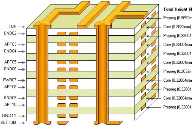
The placement of vias within the PCB stack-up is also a key consideration.
+Vias that transition between different layers can introduce impedance mismatches if not properly managed. To mitigate this, it is advisable to use blind or buried vias where possible, as these can help in maintaining a more consistent impedance profile. Additionally, ensuring that the vias are placed symmetrically and avoiding abrupt changes in the via structure can further reduce impedance variations.
Signal routing and via stitching are other important aspects to consider.
High-frequency signals are particularly sensitive to impedance discontinuities, and careful routing can help in minimizing these effects. Using controlled impedance traces and maintaining consistent trace widths and spacing can help in achieving the desired impedance levels. Via stitching, which involves placing multiple vias around a signal via, can also help in reducing impedance variations by providing a more uniform return path for the signal.
Thermal management is another factor that can impact RF impedance.
High-frequency signals can generate significant amounts of heat, which can affect the electrical properties of the materials used in the PCB. Ensuring adequate thermal management through the use of thermal vias, heat sinks, and proper PCB layout can help in maintaining consistent impedance levels and preventing signal degradation.
Finally, thorough testing and validation are essential to ensure that the designed PCB meets the desired RF impedance specifications. This involves using tools such as time-domain reflectometry (TDR) and vector network analyzers (VNA) to measure the impedance characteristics of the vias and the overall PCB. By validating the design through testing, any discrepancies can be identified and corrected before the final production.
In conclusion, managing RF impedance in multilayer PCB vias requires careful consideration of material selection, via design, placement, signal routing, thermal management, and thorough testing. By adhering to these best practices, designers can ensure that their PCBs perform optimally in high-frequency applications, maintaining signal integrity and meeting the demands of modern electronic devices.