Pcb wipe sample standards
Understanding PCB Wipe Sample Standards: A Comprehensive Guide
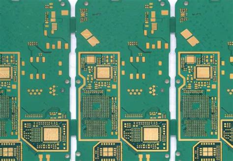
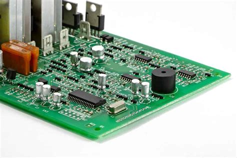
Printed Circuit Boards (PCBs) are integral components in modern electronic devices, serving as the backbone for electrical connections and functionality. As technology advances, ensuring the cleanliness and reliability of PCBs becomes increasingly critical. This is where PCB wipe sample standards come into play, providing a framework for assessing the cleanliness of PCBs to ensure optimal performance and longevity. Understanding these standards is essential for manufacturers and quality assurance professionals who aim to maintain high-quality production processes.
To begin with, PCB wipe sample standards are designed to evaluate the level of contaminants present on the surface of a PCB.
Contaminants can include dust, oils, residues from manufacturing processes, and other foreign materials that may compromise the board’s functionality. These standards provide guidelines on how to collect samples from the PCB surface and analyze them for contaminants. By adhering to these standards, manufacturers can identify potential issues early in the production process, thereby reducing the risk of product failure and enhancing the overall reliability of electronic devices.
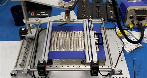
The process of collecting a PCB wipe sample typically involves using a clean, lint-free cloth or swab, which is moistened with a suitable solvent.
The cloth is then gently wiped across the surface of the PCB to collect any contaminants present. It is crucial to follow the specified procedure to ensure that the sample accurately represents the level of contamination on the board. Once the sample is collected, it is analyzed using various techniques, such as ion chromatography or mass spectrometry, to quantify the types and amounts of contaminants present.
Transitioning to the importance of these standards, it is essential to recognize that maintaining PCB cleanliness is not merely a matter of aesthetics.
Contaminants can lead to a range of issues, including electrical shorts, corrosion, and reduced thermal performance. These problems can ultimately result in device malfunction or failure, which can be costly for manufacturers and inconvenient for consumers. By implementing PCB wipe sample standards, manufacturers can proactively address these issues, ensuring that their products meet the necessary quality and reliability benchmarks.
Moreover, adherence to PCB wipe sample standards is often a requirement for compliance with industry regulations and certifications.
Many industries, such as aerospace, automotive, and medical devices, have stringent requirements for electronic components due to the critical nature of their applications. Ensuring that PCBs meet these standards is vital for manufacturers seeking to enter or remain competitive in these markets. Furthermore, compliance with these standards can enhance a company’s reputation, as it demonstrates a commitment to quality and reliability.
In addition to regulatory compliance, following PCB wipe sample standards can also lead to cost savings.
By identifying and addressing contamination issues early in the production process, manufacturers can reduce the likelihood of costly recalls or repairs. This proactive approach not only saves money but also helps maintain customer satisfaction and brand loyalty.
In conclusion, PCB wipe sample standards play a crucial role in ensuring the cleanliness and reliability of printed circuit boards. By providing a structured approach to contamination assessment, these standards help manufacturers maintain high-quality production processes, comply with industry regulations, and achieve cost savings. As technology continues to evolve, the importance of adhering to these standards will only grow, making them an indispensable tool for quality assurance in the electronics industry.
Key Benefits of Adhering to PCB Wipe Sample Standards
Adhering to PCB wipe sample standards is crucial for ensuring environmental safety and compliance with regulatory requirements. Polychlorinated biphenyls (PCBs) are synthetic organic chemicals that pose significant health risks to humans and wildlife. Consequently, the establishment and adherence to PCB wipe sample standards are essential for mitigating these risks and maintaining ecological integrity.
One of the primary benefits of adhering to these standards is the assurance of accurate and reliable data collection.
By following standardized procedures, environmental professionals can ensure that the samples collected are representative of the contamination levels present in a given area. This accuracy is vital for assessing the extent of PCB contamination and for making informed decisions regarding remediation efforts.
Moreover, compliance with PCB wipe sample standards facilitates regulatory compliance.
Various governmental agencies, such as the Environmental Protection Agency (EPA) in the United States, have established stringent guidelines for PCB management. Adhering to these standards ensures that organizations remain in compliance with legal requirements, thereby avoiding potential fines and legal repercussions. Furthermore, regulatory compliance demonstrates a commitment to environmental stewardship, which can enhance an organization’s reputation and foster trust among stakeholders.
In addition to regulatory compliance, adhering to PCB wipe sample standards can lead to cost savings.
By ensuring accurate data collection and analysis, organizations can avoid unnecessary remediation efforts that may arise from inaccurate or inconsistent sampling methods. This precision allows for targeted remediation strategies, which can be more cost-effective than broad, unfocused approaches. Additionally, by preventing regulatory fines and potential litigation, organizations can allocate resources more efficiently towards environmental management and sustainability initiatives.
Another significant benefit of adhering to PCB wipe sample standards is the protection of public health.
PCBs are known to cause a range of adverse health effects, including cancer, immune system suppression, and neurological damage. By accurately assessing and addressing PCB contamination, organizations can reduce the risk of exposure to these harmful chemicals. This proactive approach not only protects the health of individuals in affected areas but also contributes to the overall well-being of communities.
Furthermore, adherence to PCB wipe sample standards supports environmental conservation efforts.
PCBs are persistent in the environment and can accumulate in the food chain, posing a threat to wildlife and ecosystems. By accurately identifying and mitigating PCB contamination, organizations can help preserve biodiversity and protect natural habitats. This commitment to environmental conservation aligns with global sustainability goals and contributes to the long-term health of the planet.
In conclusion, the key benefits of adhering to PCB wipe sample standards are multifaceted, encompassing accurate data collection, regulatory compliance, cost savings, public health protection, and environmental conservation. By following these standards, organizations can effectively manage PCB contamination, thereby safeguarding human health and the environment. As awareness of environmental issues continues to grow, the importance of adhering to these standards will only increase, underscoring the need for ongoing commitment to best practices in environmental management. Through diligent adherence to PCB wipe sample standards, organizations can play a pivotal role in promoting a safer and more sustainable future for all.
Common Challenges in Implementing PCB Wipe Sample Standards
Implementing PCB wipe sample standards presents a range of challenges that organizations must navigate to ensure compliance and accuracy. Polychlorinated biphenyls (PCBs) are hazardous chemical compounds that were widely used in industrial applications until their ban in many countries due to environmental and health concerns. Consequently, the need for effective monitoring and remediation of PCB contamination has become paramount. However, establishing and adhering to PCB wipe sample standards is fraught with complexities.
One of the primary challenges in implementing these standards is the variability in contamination levels across different sites.
PCB contamination can vary significantly depending on factors such as historical usage, environmental conditions, and the nature of the materials involved. This variability necessitates a flexible yet robust approach to sampling, which can be difficult to standardize. Moreover, the lack of uniformity in contamination levels can lead to discrepancies in sample results, complicating the interpretation and comparison of data across different locations.
In addition to variability, the technical aspects of sampling and analysis pose significant hurdles.
The process of collecting wipe samples requires meticulous attention to detail to avoid cross-contamination and ensure the integrity of the samples. This involves using appropriate materials and techniques, which can vary depending on the specific standards being followed. Furthermore, the analytical methods used to detect and quantify PCBs must be sensitive and precise, often requiring sophisticated laboratory equipment and expertise. The complexity of these technical requirements can be a barrier for organizations with limited resources or access to specialized facilities.
Another challenge is the regulatory landscape surrounding PCB wipe sample standards.
Regulations can differ widely between jurisdictions, leading to confusion and inconsistency in implementation. Organizations operating in multiple regions may find it particularly challenging to navigate these differences and ensure compliance with all applicable standards. Additionally, regulatory updates and changes can occur, necessitating continuous monitoring and adaptation of sampling protocols. This dynamic regulatory environment requires organizations to remain vigilant and proactive in their approach to PCB sampling.
Furthermore, the cost implications of implementing PCB wipe sample standards cannot be overlooked.
The expenses associated with sampling, analysis, and compliance can be substantial, particularly for large-scale operations or sites with extensive contamination. Organizations must balance the need for thorough monitoring with budgetary constraints, which can be a delicate and challenging task. Cost considerations may also influence the frequency and scope of sampling, potentially impacting the overall effectiveness of contamination assessment and remediation efforts.
Despite these challenges, there are strategies that organizations can employ to facilitate the implementation of PCB wipe sample standards.
Collaboration with experienced environmental consultants and laboratories can provide valuable expertise and resources, helping to ensure that sampling and analysis are conducted accurately and efficiently. Additionally, investing in training and education for personnel involved in sampling can enhance the quality and reliability of the data collected. By fostering a culture of continuous improvement and staying informed about regulatory developments, organizations can better navigate the complexities of PCB wipe sample standards.
In conclusion, while the implementation of PCB wipe sample standards is fraught with challenges, it is a critical component of effective environmental management and compliance. By understanding and addressing the variability in contamination levels, technical complexities, regulatory differences, and cost considerations, organizations can develop robust strategies to overcome these obstacles. Through collaboration, training, and a commitment to continuous improvement, the successful implementation of PCB wipe sample standards is achievable, ultimately contributing to the protection of human health and the environment.
Innovations in PCB Wipe Sample Standards and Their Impact on Industry Practices
In recent years, the field of printed circuit board (PCB) manufacturing has witnessed significant advancements, particularly in the realm of PCB wipe sample standards. These standards are crucial for ensuring the cleanliness and quality of PCBs, which are integral components in a wide array of electronic devices. As the demand for more reliable and efficient electronic products continues to grow, the importance of maintaining stringent cleanliness standards in PCB manufacturing cannot be overstated. Consequently, innovations in PCB wipe sample standards have emerged as a pivotal factor in enhancing industry practices.
To begin with, PCB wipe sample standards are designed to assess the level of contaminants present on the surface of PCBs.
These contaminants, which can include dust, oils, and other residues, have the potential to compromise the functionality and longevity of electronic devices. Therefore, maintaining a high level of cleanliness is essential to prevent failures and ensure optimal performance. Traditionally, the methods used to evaluate PCB cleanliness involved manual inspections and basic testing techniques. However, these methods often lacked precision and consistency, leading to variability in results.
In response to these challenges, recent innovations have introduced more sophisticated and reliable techniques for PCB wipe sampling.
One such advancement is the development of automated systems that utilize advanced sensors and imaging technologies to detect and quantify contaminants with greater accuracy. These systems not only enhance the precision of cleanliness assessments but also streamline the testing process, allowing for faster and more efficient evaluations. As a result, manufacturers can ensure that their PCBs meet the required standards without compromising on production timelines.
Moreover, the integration of data analytics into PCB wipe sample standards has further revolutionized industry practices.
By leveraging big data and machine learning algorithms, manufacturers can now analyze vast amounts of data collected from wipe samples to identify patterns and trends in contamination levels. This data-driven approach enables manufacturers to implement proactive measures to mitigate contamination risks, thereby improving the overall quality of their products. Additionally, the insights gained from data analytics can inform the development of more targeted and effective cleaning protocols, further enhancing the cleanliness of PCBs.
Another noteworthy innovation in PCB wipe sample standards is the adoption of environmentally friendly practices.
As sustainability becomes an increasingly important consideration in manufacturing, there is a growing emphasis on reducing the environmental impact of PCB production processes. To this end, new standards have been established to promote the use of eco-friendly cleaning agents and materials in wipe sampling procedures. These standards not only help minimize the ecological footprint of PCB manufacturing but also align with the broader industry trend towards sustainable practices.
In conclusion, the innovations in PCB wipe sample standards have had a profound impact on industry practices, driving improvements in both the quality and sustainability of PCB manufacturing. By embracing advanced technologies, data analytics, and environmentally conscious practices, manufacturers are better equipped to meet the evolving demands of the electronics market. As these innovations continue to evolve, they will undoubtedly play a crucial role in shaping the future of PCB manufacturing, ensuring that electronic devices remain reliable, efficient, and sustainable. Through these advancements, the industry is poised to achieve new heights in quality assurance and environmental responsibility, ultimately benefiting both manufacturers and consumers alike.