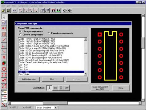
Pcb wipe sample units
Benefits Of Using PCB Wipe Sample Units In Quality Control
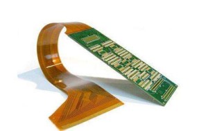
Printed Circuit Boards (PCBs) are integral components in modern electronic devices, and ensuring their quality is paramount for manufacturers. One effective method for maintaining high standards in PCB production is the use of PCB wipe sample units. These units offer numerous benefits in quality control, enhancing the reliability and performance of electronic products. By examining the advantages of PCB wipe sample units, it becomes evident why they are indispensable in the manufacturing process.
Firstly, PCB wipe sample units provide a precise and efficient means of detecting contaminants on the surface of PCBs.
Contaminants such as dust, oils, and residues can significantly impact the functionality of electronic components. By utilizing wipe sample units, manufacturers can identify and address these contaminants early in the production process. This proactive approach not only prevents potential defects but also reduces the likelihood of costly recalls and repairs. Consequently, the use of PCB wipe sample units contributes to the overall reliability and longevity of electronic devices.
In addition to detecting contaminants, PCB wipe sample units play a crucial role in ensuring compliance with industry standards and regulations.
The electronics industry is governed by stringent quality control standards, such as the IPC-A-610 standard, which outlines the acceptability of electronic assemblies. By employing PCB wipe sample units, manufacturers can verify that their products meet these standards, thereby avoiding non-compliance issues and potential penalties. This adherence to industry standards not only enhances the reputation of the manufacturer but also instills confidence in consumers regarding the quality of the products they purchase.
Moreover, PCB wipe sample units facilitate the identification of process inefficiencies and areas for improvement within the manufacturing workflow.
By regularly analyzing wipe samples, manufacturers can gain valuable insights into the effectiveness of their cleaning and handling procedures. For instance, if a high level of contaminants is consistently detected, it may indicate a need for improved cleaning protocols or better environmental controls. Addressing these inefficiencies can lead to more streamlined production processes, reduced waste, and ultimately, cost savings for the manufacturer.
Furthermore, the use of PCB wipe sample units can enhance traceability and accountability in the production process.
Each wipe sample can be documented and tracked, providing a comprehensive record of the cleanliness and quality of PCBs at various stages of production. This traceability is particularly valuable in the event of a quality issue or product failure, as it allows manufacturers to pinpoint the source of the problem and implement corrective actions. Additionally, maintaining detailed records of wipe sample results can serve as evidence of due diligence in quality control, which is beneficial in audits and customer inquiries.
Another significant benefit of PCB wipe sample units is their contribution to continuous improvement initiatives.
By systematically collecting and analyzing data from wipe samples, manufacturers can identify trends and patterns that may indicate underlying issues or opportunities for enhancement. This data-driven approach enables manufacturers to make informed decisions and implement targeted improvements, fostering a culture of continuous improvement within the organization. Over time, these incremental improvements can lead to substantial gains in product quality and operational efficiency.
In conclusion, the use of PCB wipe sample units in quality control offers a multitude of benefits for manufacturers. From detecting contaminants and ensuring compliance with industry standards to identifying process inefficiencies and enhancing traceability, these units play a vital role in maintaining the quality and reliability of electronic products. By leveraging the insights gained from wipe sample analysis, manufacturers can drive continuous improvement and achieve long-term success in the competitive electronics market.
How To Properly Utilize PCB Wipe Sample Units For Accurate Results
Proper utilization of PCB wipe sample units is essential for obtaining accurate results in environmental testing and contamination assessment. Polychlorinated biphenyls (PCBs) are hazardous chemical compounds that were widely used in various industrial applications until their ban due to health and environmental concerns. Consequently, detecting and quantifying PCB contamination in different environments is crucial for ensuring safety and compliance with regulatory standards. To achieve reliable results, it is imperative to follow a systematic approach when using PCB wipe sample units.
First and foremost, selecting the appropriate sampling materials is critical.
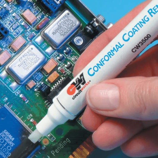
PCB wipe sample units typically consist of pre-moistened wipes, which are designed to effectively capture PCB residues from surfaces. It is important to ensure that the wipes are compatible with the specific type of surface being tested, as different materials may require different types of wipes to achieve optimal results. Additionally, the wipes should be free from any contaminants that could interfere with the analysis.
Before commencing the sampling process, it is essential to wear appropriate personal protective equipment (PPE) to prevent exposure to PCBs and other hazardous substances. This includes gloves, safety goggles, and protective clothing. Ensuring that the sampling area is well-ventilated can further minimize the risk of inhaling any airborne contaminants.
The next step involves preparing the sampling area.
It is advisable to delineate the area to be sampled using a template or marking tape to ensure consistency and accuracy. The size of the sampling area should be standardized, typically around 100 square centimeters, to facilitate comparison of results across different samples. Cleaning the sampling area with a solvent that does not interfere with PCB analysis can help remove any loose debris or contaminants that may affect the accuracy of the results.
When performing the wipe sampling, it is important to follow a consistent technique.
The wipe should be unfolded and held flat against the surface, applying even pressure to ensure thorough contact. Wiping should be done in a systematic manner, typically using a horizontal and vertical motion to cover the entire sampling area. It is crucial to avoid overlapping or missing any sections of the area to ensure that the sample is representative of the entire surface.
After completing the wipe sampling, the wipe should be carefully folded with the sampled side inward to prevent contamination.
The wipe should then be placed in a clean, labeled container, such as a glass jar or a polyethylene bag, to preserve the integrity of the sample. Proper labeling is essential, including details such as the date, time, location, and any other relevant information that can aid in the analysis and interpretation of the results.
Transporting the samples to the laboratory should be done promptly and under appropriate conditions to prevent any degradation or contamination. It is advisable to use coolers or insulated containers to maintain a stable temperature during transit. Upon arrival at the laboratory, the samples should be stored in a controlled environment until analysis.
In conclusion, the accurate utilization of PCB wipe sample units requires careful attention to detail and adherence to standardized procedures. By selecting the appropriate materials, wearing proper PPE, preparing the sampling area, following a consistent wiping technique, and ensuring proper sample handling and transportation, one can obtain reliable and accurate results. These results are crucial for assessing PCB contamination and making informed decisions to protect human health and the environment.
Common Mistakes To Avoid When Handling PCB Wipe Sample Units
When handling PCB wipe sample units, it is crucial to adhere to best practices to ensure the accuracy and reliability of the results. One common mistake is the improper selection of sampling materials. Using non-approved or contaminated wipes can introduce extraneous substances that may skew the results. Therefore, it is essential to use only those materials that meet the specific requirements for PCB sampling, ensuring they are clean and free from any contaminants.
Another frequent error involves inadequate preparation of the sampling area.
Before collecting samples, the area should be thoroughly cleaned to remove any dust, dirt, or other potential contaminants. Failure to do so can result in the collection of extraneous materials, which can compromise the integrity of the sample. Additionally, it is important to avoid touching the sampling area with bare hands, as oils and residues from the skin can also contaminate the sample.
Proper labeling and documentation are also critical aspects that are often overlooked.
Each sample must be clearly labeled with relevant information, including the date, time, location, and any other pertinent details. Inadequate labeling can lead to confusion and potential mix-ups, which can invalidate the results. Furthermore, maintaining a detailed log of the sampling process, including any observations or deviations from standard procedures, is essential for traceability and quality control.
Handling and storage of the samples post-collection is another area where mistakes are commonly made.
Samples should be stored in clean, airtight containers to prevent contamination and degradation. It is also important to keep the samples at a stable temperature, as fluctuations can affect the integrity of the sample. Mishandling or improper storage can lead to compromised results, rendering the entire sampling effort futile.
Another critical mistake to avoid is the failure to calibrate and maintain sampling equipment.
Regular calibration ensures that the equipment is functioning correctly and providing accurate readings. Neglecting this step can result in erroneous data, which can have significant implications for the analysis. Additionally, routine maintenance of the equipment is necessary to prevent malfunctions and ensure consistent performance.
Moreover, it is essential to follow the prescribed sampling protocol meticulously.
Deviating from the established procedures can introduce variables that may affect the outcome of the analysis. This includes adhering to the specified number of wipes, the pressure applied during sampling, and the duration of the wiping process. Consistency in following the protocol ensures that the samples are representative and comparable.
Lastly, it is important to be aware of and comply with all relevant regulations and guidelines governing PCB sampling.
Non-compliance can not only lead to invalid results but also legal repercussions. Staying informed about the latest standards and best practices is crucial for ensuring that the sampling process is conducted correctly and ethically.
In conclusion, handling PCB wipe sample units requires careful attention to detail and adherence to established protocols. By avoiding common mistakes such as improper selection of materials, inadequate preparation, poor labeling, mishandling of samples, neglecting equipment maintenance, deviating from protocols, and non-compliance with regulations, one can ensure the accuracy and reliability of the results. Through diligent practice and continuous improvement, the integrity of PCB sampling can be maintained, providing valuable data for environmental and health assessments.
Innovations In PCB Wipe Sample Units For Enhanced Performance
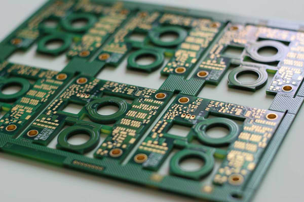
Printed Circuit Boards (PCBs) are integral components in modern electronic devices, and their cleanliness is paramount to ensuring optimal performance and longevity. Innovations in PCB wipe sample units have significantly enhanced the ability to maintain and verify the cleanliness of these critical components. These advancements are crucial for industries where even the slightest contamination can lead to substantial operational failures or inefficiencies.
One of the primary innovations in PCB wipe sample units is the development of more sensitive and accurate detection methods.
Traditional methods often relied on visual inspections or basic chemical tests, which could miss minute contaminants. However, modern units employ advanced technologies such as ion chromatography and mass spectrometry. These techniques allow for the detection of trace amounts of ionic and organic contaminants, providing a more comprehensive analysis of the PCB’s cleanliness. Consequently, this ensures that even the smallest particles, which could potentially cause short circuits or corrosion, are identified and addressed.
In addition to improved detection capabilities, the design of PCB wipe sample units has also seen significant enhancements.
Contemporary units are more ergonomic and user-friendly, facilitating easier handling and more efficient sampling processes. This is particularly important in high-volume manufacturing environments where speed and accuracy are critical. The integration of automated systems within these units further streamlines the sampling process, reducing the likelihood of human error and ensuring consistent results. Automation also allows for the collection of large datasets, which can be analyzed to identify trends and potential issues before they become critical.
Moreover, the materials used in PCB wipe sample units have evolved to provide better performance.
High-purity solvents and specialized wipe materials are now standard, minimizing the risk of introducing additional contaminants during the sampling process. These materials are designed to be non-abrasive, ensuring that the integrity of the PCB surface is maintained while effectively removing contaminants. The use of such high-quality materials is essential in industries like aerospace and medical devices, where the highest standards of cleanliness are mandatory.
Another significant innovation is the incorporation of real-time monitoring and data logging capabilities.
Modern PCB wipe sample units can now be connected to centralized monitoring systems, allowing for continuous tracking of cleanliness levels. This real-time data is invaluable for quality control and can be used to make immediate adjustments to the manufacturing process if contamination levels exceed acceptable thresholds. Furthermore, the ability to log and analyze historical data provides insights into long-term trends and helps in the development of more effective cleaning protocols.
The environmental impact of PCB wipe sample units has also been a focus of recent innovations.
Manufacturers are increasingly adopting eco-friendly practices, such as using biodegradable solvents and recyclable materials. These efforts not only reduce the environmental footprint of the sampling process but also align with broader industry trends towards sustainability. By minimizing waste and reducing the use of hazardous chemicals, these innovations contribute to a more sustainable manufacturing ecosystem.
In conclusion, the advancements in PCB wipe sample units have significantly enhanced their performance, making them more accurate, efficient, and environmentally friendly. These innovations are crucial for maintaining the cleanliness and reliability of PCBs, which are essential for the proper functioning of modern electronic devices. As technology continues to evolve, it is likely that further improvements will be made, ensuring that PCB wipe sample units remain at the forefront of quality control in the electronics industry.