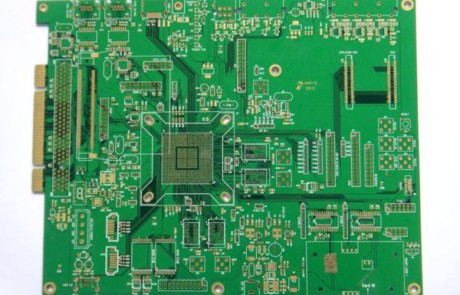
PCB wiring skills and essentials
Wiring is an important part of the PCB design process. All the preliminary preparations are done for it. In the entire PCB design process, the design process of wiring is the most delicate and the most limited. PCB wiring has single-sided, double-sided and multi-layer wiring.
There are two ways: automatic and interactive wiring. Before automatic wiring, you can use interactive wiring to pre-wire the lines with higher requirements. The edge lines of the input and output ends should not be adjacent and parallel to avoid reflection interference.
If necessary, a ground wire can be added for isolation, and the wiring of two adjacent layers should be perpendicular to each other, because parallel wiring is more likely to produce parasitic coupling.
The routing rate of automatic wiring depends on a good layout, and wiring rules can be set in advance, such as the number of bending times, the number of vias, the number of steps, etc. Generally, exploratory wiring is performed first to quickly connect short lines, and then the maze wiring is used to optimize the global wiring path of the lines to be routed. It can disconnect the wires that have been routed as needed and try to re-route them, thereby improving the overall wiring effect.
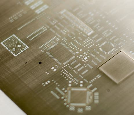
Through holes are no longer suitable for the current high-density PCB design.
It wastes a lot of precious wiring channels. In order to solve this problem, blind and buried hole technologies have emerged. It not only completes the role of the through hole, but also saves a lot of wiring channels, making the wiring process smoother, more convenient and perfect. If you want to master the design of PCB boards, you need to do more hands-on work and understand its true meaning through personal experience. In addition to PCB copying, I will analyze the skills and essentials of PCB wiring for everyone.
1.Processing of power supply and ground wires
Although the wiring of the entire PCB board is well completed, it is still necessary to consider the interference caused by the power supply and ground wire, which will reduce the performance of the product and even affect the success rate of the product. Therefore, the wiring of the power supply and ground wire should be taken seriously, and the interference caused by the power supply and ground wire should be minimized to ensure product quality.
Every engineer engaged in electronic product design understands why interference between the power supply line and the ground wire occurs. Now only the reduction type suppression of interference is described.
Decoupling capacitors should be added between the power supply and the ground wire.
Try to widen the power and ground wires.
It is best that the ground wire is wider than the power wire. The relationship is: ground wire > power wire > signal wire. The usual signal wire width is: 0.2~0.3mm, the thinnest width can reach 0.05~0.07mm, and the power wire is 1.2~2.5mm.
The PCB design of digital circuits can use a wider ground wire to form a loop and a ground network for use, but remember that the ground of analog circuits cannot be used in this way.
Use a large area of copper layer as a ground wire, connect all unused areas on the printed circuit board to the ground, use it as a ground wire or make a multi-layer board, with the power supply and ground wire occupying one layer each.
2.Common ground processing of digital circuits and analog circuits
Now, many PCBs are no longer single-function circuits, but are composed of a mixture of digital circuits and analog circuits. Therefore, when wiring, it is necessary to consider the problem of mutual interference between them, especially the noise interference on the ground wire.
Digital circuits have high frequencies and analog circuits are highly sensitive.
For signal lines, high-frequency signal lines should be as far away from sensitive analog circuit devices as possible. For ground lines, the entire PCB can only have one node to the outside world, so the problem of common ground for digital circuits and analog circuits must be handled inside the PCB. Inside the circuit board, the ground of the digital circuit and the ground of the analog circuit are actually separated, only at the interface where the PCB is connected to the outside world (such as plugs, etc.). The ground of the digital circuit and the ground of the analog circuit are a little short-circuited. Please note that there is only one connection point, and there are also non-common grounds on the PCB, which is determined by the system design.
3.Signal lines are laid on the power (ground) layer
When wiring a multi-layer printed circuit board, since there are not many lines left in the signal line layer, adding more layers will cause waste, and will also increase the workload and cost. You can consider wiring on the power (ground) layer. First, you should consider using the power layer, and then the ground layer, because it can best preserve the integrity of the ground layer.


