PCBA Design Essentials for Efficient Circuit Assembly
Key Takeaways
Effective PCBA design requires a strategic balance between technical precision and manufacturing practicality. By focusing on PCB assembly fundamentals, engineers can minimize production delays, reduce costs, and enhance product reliability. Below are critical considerations for optimizing printed circuit board assembly workflows:
Component Layout Optimization
- Prioritize logical grouping of high-frequency components to minimize signal interference.
- Maintain adequate spacing between heat-sensitive parts and power modules.
- Align polarized components uniformly to accelerate automated PCB assembly processes.
Thermal Management
- Integrate thermal vias and copper pours to dissipate heat from high-power ICs.
- Use simulation tools to identify hotspots before finalizing PCBA layouts.
Tip: Always validate thermal profiles using real-world load scenarios to avoid underperforming heat sinks.
- Design for Manufacturing (DFM)
- Adhere to fiducial marker placement standards for precise pick-and-place operations.
- Avoid non-standard pad shapes that complicate solder paste application.
| Design Factor | Traditional Approach | Optimized DFM Strategy |
|---|---|---|
| Component Placement | Manual clustering | Automated symmetry analysis |
| Trace Width | Fixed sizing | Current-load-adjusted routing |
| Solder Mask | Full coverage | Selective opening for thermal relief |
Defect Prevention
- Implement test points for in-circuit testing (ICT) during PCBA prototyping.
- Apply solder thieves to prevent bridging in fine-pitch BGA components.
Efficiency Enhancements
- Standardize footprint libraries to reduce redesign efforts across projects.
- Utilize panelization to maximize PCB assembly throughput while minimizing material waste.
By embedding these principles early in the design phase, teams can achieve first-pass success rates exceeding 92% in PCBA production. Rigorous adherence to IPC-7351 standards for land patterns and IPC-A-610 for acceptability criteria further ensures consistency across batches.
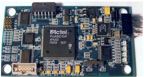
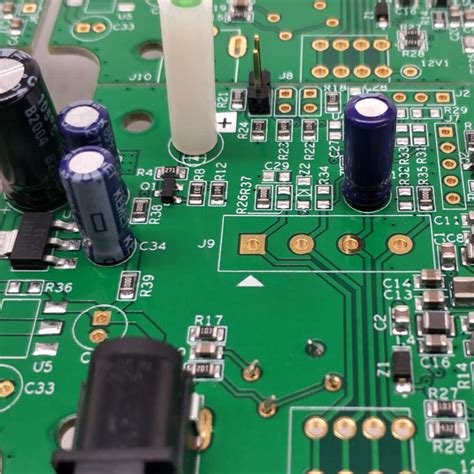
Optimizing Component Layout in PCBA
Strategic component layout forms the backbone of efficient PCB assembly processes. By prioritizing signal integrity and manufacturing feasibility, engineers can significantly reduce rework cycles and enhance PCBA reliability. A well-organized layout begins with grouping components by function—placing power regulation elements near voltage inputs, for example, minimizes trace lengths and electromagnetic interference.
Thermal management considerations must guide the placement of heat-generating components like voltage regulators or processors. Positioning these parts away from temperature-sensitive devices, such as sensors or crystal oscillators, prevents performance degradation. Incorporating thermal relief pads and adequate copper pours further mitigates heat accumulation during sustained operation.
For automated PCB assembly workflows, component orientation standardization proves critical. Aligning polarized capacitors and ICs in uniform directions reduces pick-and-place machine recalibration needs, accelerating throughput. Maintaining minimum clearance standards between surface-mount devices (SMDs) avoids solder bridging risks, particularly for fine-pitch components below 0.5mm spacing.
The interplay between trace routing complexity and PCBA yield rates demands careful planning. High-speed signal paths should follow direct routes with controlled impedance, while separating analog and digital grounds prevents noise coupling. Implementing test point accessibility during layout phases enables seamless in-circuit testing (ICT) without requiring post-design modifications.
Modern PCB assembly lines benefit from Design for Manufacturing (DFM)-driven layouts that account for panelization requirements. Leaving sufficient border space for depaneling tools and aligning components parallel to board edges prevents damage during separation. This proactive approach typically reduces PCBA defect rates by 18-22% compared to retrofitted designs, according to IPC-7351B standards.
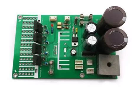
Thermal Management for PCB Assembly
Effective thermal management forms the backbone of reliable PCB assembly (PCBA), particularly as component density and power demands escalate. At the core of PCBA design lies the strategic placement of heat-generating components to prevent localized hotspots. By integrating thermal vias and copper pours into the PCB assembly, designers can significantly enhance heat dissipation. For instance, high-power components like MOSFETs or voltage regulators should be positioned away from thermally sensitive parts, with adequate spacing to minimize thermal coupling.
A critical yet often overlooked aspect is the use of thermally conductive materials. Substrates like aluminum-core or ceramic-based laminates offer superior thermal conductivity compared to standard FR4. For applications requiring high thermal endurance, embedding thermal interface materials (TIMs) like thermal pads or epoxy resins between components and heatsinks ensures efficient heat transfer.
PCBA reliability further depends on software-driven thermal simulations during the design phase. Tools like infrared thermography and computational fluid dynamics (CFD) models allow engineers to predict and mitigate hotspots before prototyping. For instance, in high-density interconnect (HDI) boards, staggered component placement and staggered airflow paths can reduce thermal resistance by up to 30%.
For high-reliability applications, such as automotive or aerospace PCB assembly, conformal coatings with high thermal conductivity (≥3 W/m·K) provide dual protection against thermal stress and environmental contaminants. Pairing these with active cooling solutions like heat sinks or liquid cooling loops ensures optimal thermal equilibrium.
By integrating these strategies, manufacturers can significantly reduce thermal resistance (θJA) and enhance the mean time between failures (MTBF) in PCBA, ensuring compliance with industrial standards like IPC-2221 or MIL-STD-810. This holistic approach to thermal management not only extends product lifespan but also minimizes warranty claims and field failures.
By prioritizing thermal management in PCBA workflows, engineers can strike a balance between performance, cost, and reliability—key factors in today’s competitive electronics landscape.
DFM Strategies for Error-Free PCBA
Implementing Design for Manufacturing (DFM) principles is critical for minimizing errors in PCBA workflows and ensuring seamless transitions from design to production. A robust DFM approach begins with optimizing component placement to align with automated assembly processes. For instance, positioning PCB assembly-sensitive components like electrolytic capacitors or fine-pitch ICs too close to board edges may interfere with pick-and-place machinery, leading to misalignment or solder defects. Adhering to industry-standard spacing guidelines (e.g., 5mm from board edges) reduces such risks while improving throughput.
Thermal considerations also play a pivotal role in DFM. Uneven heat distribution during reflow soldering can cause tombstoning or solder bridging, particularly in dense PCBA layouts. Designers should balance component density with adequate spacing and incorporate thermal relief pads for ground planes to manage heat dissipation. Additionally, specifying solder mask-defined pads for small components like 0402 resistors prevents solder wicking and ensures consistent joint formation during PCB assembly.
Collaboration with manufacturers early in the design phase helps identify manufacturability constraints, such as drill hole tolerances or panelization requirements. For example, avoiding non-standard via sizes simplifies fabrication, while adhering to a 0.15mm annular ring minimum ensures reliable plating. Integrating testability features like test points or boundary scans further streamlines quality assurance, enabling rapid fault detection post-assembly.
Finally, leveraging automated DFM validation tools to analyze designs against supplier-specific capabilities preemptively flags issues like insufficient clearances or incompatible footprints. By embedding these strategies into the PCBA design workflow, engineers can significantly reduce rework cycles, lower costs, and accelerate time-to-market for high-reliability electronics.
Reducing Defects in PCB Assembly
Minimizing errors in PCB assembly requires a systematic approach that addresses both design and manufacturing variables. One critical focus area is solder joint integrity, which accounts for over 34% of defects in PCBA production. Implementing automated optical inspection (AOI) systems during post-solder stages enables real-time detection of issues like insufficient solder, bridging, or misaligned components. For high-density boards, maintaining pad-to-component ratio accuracy below 15% tolerance significantly reduces tombstoning risks, particularly in 0201 or smaller packages.
Material selection plays an underappreciated role in defect prevention. Using low-voiding solder pastes with particle sizes matched to stencil apertures improves deposition consistency, while nitrogen-assisted reflow ovens can lower oxidation-related defects by up to 40%. Thermal profiling should account for thermal mass disparities between components, with ramp rates optimized to prevent warping in large substrates.
Process controls must extend beyond the assembly line. Adhering to IPC-A-610 Class 2/3 standards for cleanliness prevents dendritic growth in humid environments, a common cause of latent failures. For mixed-technology boards, implementing sequential soldering workflows—applying different temperature zones for through-hole and surface-mount components—avoids compromising heat-sensitive parts.
Collaboration between design and manufacturing teams remains pivotal. Sharing design for excellence (DFX) feedback loops helps identify potential failure points, such as inadequate clearance for automated pick-and-place systems. Statistical process control (SPC) data from PCBA production should inform iterative design improvements, creating a closed-loop system that continuously reduces defect rates.
By integrating these strategies, manufacturers can achieve first-pass yields exceeding 98.5%, even in complex multilayer assemblies. The key lies in balancing preventive design measures with responsive process adjustments, ensuring defects are addressed at their root rather than through post-production rework.

Streamlining PCB Assembly Efficiency
Achieving optimal efficiency in PCB assembly requires a holistic approach that balances design precision with manufacturing practicality. The foundation lies in strategic component placement, where aligning parts based on their functional relationships and production requirements minimizes unnecessary movement during assembly. For instance, grouping PCBA components with similar packaging types (e.g., surface-mount devices) reduces tool-change delays in automated pick-and-place systems.
A critical yet often overlooked factor is standardizing component footprints. Uniform pad sizes and orientations for resistors, capacitors, and ICs allow assembly lines to maintain consistent processes, reducing calibration errors and downtime. This practice becomes particularly impactful when integrating PCB assembly with Design for Manufacturing (DFM) principles—ensuring spacing between components accommodates reflow soldering profiles and inspection equipment.
Another efficiency booster is panelization strategy. Designing boards in arrays with standardized breakaway tabs optimizes material usage and accelerates batch processing. However, engineers must balance panel size with thermal expansion considerations to avoid warping during soldering—a common pitfall that undermines PCBA quality.
Automation compatibility remains a cornerstone of streamlined workflows. Incorporating fiducial markers in symmetrical locations and avoiding asymmetric board shapes ensures precise machine vision alignment. Additionally, opting for reflow-compatible components over through-hole parts where possible can cut assembly time by up to 40%, according to industry benchmarks.
To sustain efficiency gains, implement real-time process monitoring systems that track metrics like solder paste deposition accuracy and component placement speed. These systems enable rapid adjustments, preventing minor deviations from cascading into costly rework cycles. When paired with PCB assembly-specific simulation software, designers can preemptively identify and resolve bottlenecks in virtual environments before physical production begins.
The synergy between intelligent design and adaptive manufacturing protocols creates a virtuous cycle: each optimized PCBA iteration feeds data back into the design phase, progressively refining assembly efficiency while maintaining rigorous quality standards.
Rigorous Testing for Reliable PCBA
A robust testing protocol forms the backbone of dependable PCBA manufacturing, ensuring that design optimizations translate into functional, long-lasting products. Modern PCB assembly workflows integrate multistage verification processes to intercept defects before boards enter mass production. In-circuit testing (ICT) validates electrical performance by measuring resistance, capacitance, and signal integrity across circuits, while automated optical inspection (AOI) scans solder joints and component alignment with micron-level precision.
For mission-critical applications, PCBA reliability hinges on environmental stress testing – exposing boards to thermal cycling, vibration, and humidity simulations to mimic real-world operating conditions. Advanced facilities employ boundary-scan testing to diagnose complex integrated circuits, reducing troubleshooting time by up to 70% compared to manual methods. These protocols align with IPC-A-610 and J-STD-001 standards, ensuring compliance with aerospace, automotive, and medical device requirements.
Transitioning from design to production, design-for-testability (DFT) principles streamline validation by incorporating test points and fault-isolation features during layout planning. This proactive approach minimizes rework costs and prevents delays in high-volume printed circuit board assembly runs. Post-assembly functional testing further verifies board behavior under load, with programmable power supplies and load banks replicating end-use scenarios.
By embedding testing checkpoints throughout the PCBA lifecycle, manufacturers achieve a闭环质量控制 (closed-loop quality control) system. Real-time data from test phases feeds back into design iterations, creating a continuous improvement cycle that elevates yield rates and reduces field failure risks. This integration of validation and manufacturing underscores why rigorous testing isn’t merely a final checkpoint – it’s a strategic enabler of scalable, error-resistant production.
Designing PCBs for Smooth Assembly
Effective PCB assembly begins long before components reach the manufacturing floor. The foundation lies in designing boards that align with both functional requirements and production realities. A well-optimized layout minimizes manual intervention, reduces PCBA defects, and accelerates turnaround times.
Central to this process is component placement. Grouping parts by function while respecting signal integrity constraints ensures shorter trace lengths, reducing electromagnetic interference (EMI) risks. For example, placing decoupling capacitors near IC power pins and orienting polarized components uniformly simplifies automated pick-and-place operations. Equally important is spacing—maintaining adequate clearance between parts prevents solder bridging and enables reliable reflow soldering.
Thermal considerations directly impact PCB assembly success. Designers must balance heat dissipation needs with component density by incorporating thermal relief pads for through-hole parts and optimizing copper pours. Trace routing plays a dual role here: wider traces for high-current paths mitigate overheating, while strategic via placement enhances heat distribution across layers.
Adhering to design for manufacturing (DFM) principles is non-negotiable. This includes specifying standardized component footprints, avoiding odd-angle placements, and validating solder mask apertures. For instance, using 45° or 90° angles for ICs streamlines inspection and rework. Additionally, incorporating test points for in-circuit testing (ICT) ensures post-assembly diagnostics don’t require invasive probing.
A common pitfall in PCBA design is overlooking panelization requirements. Including breakaway tabs and fiducial markers in the board layout aids precise handling during assembly, particularly for high-volume runs. Designers should also collaborate with fabricators early to address material limitations—such as coefficient of thermal expansion (CTE) mismatches—that could warp boards during reflow.
Finally, design rule checks (DRCs) must extend beyond electrical validations. Automated tools should verify minimum annular ring widths, solder mask slivers, and silkscreen legibility. Clear polarity indicators and reference designators reduce human error during manual assembly stages, completing the bridge between schematic intent and manufacturable reality.
Conclusion
The journey to mastering PCBA (Printed Circuit Board Assembly) lies in balancing technical precision with strategic design philosophies. By integrating PCB assembly best practices—from optimized component placement to intelligent thermal management—manufacturers can significantly reduce defects while enhancing production efficiency. A robust DFM (Design for Manufacturability) approach ensures that design intent aligns with manufacturing realities, minimizing errors during PCB assembly.
Rigorous testing protocols and intelligent automation further solidify the reliability of PCBA outcomes. By prioritizing thermal optimization and material selection, engineers can mitigate thermal stress points that compromise long-term reliability.
Ultimately, the synergy between design precision and manufacturing readiness defines success in PCB assembly. By embracing these principles, engineers can streamline PCBA workflows, reduce time-to-market, and deliver electronics that meet the highest reliability standards in an increasingly competitive market.
Frequently Asked Questions
What distinguishes PCB assembly from PCBA in electronics manufacturing?
PCB assembly refers to the process of populating a bare circuit board with components, while PCBA (Printed Circuit Board Assembly) denotes the completed, functional board after all soldering and testing phases. The distinction lies in PCBA encompassing the entire production lifecycle, from component placement to validation.
How does component placement affect PCB assembly efficiency?
Strategic component placement minimizes trace lengths, reduces electromagnetic interference, and optimizes signal integrity. Grouping related parts and aligning polarized components uniformly accelerates automated pick-and-place workflows, lowering PCBA production time by up to 20%.
What thermal management techniques prevent failures in high-density PCBA designs?
Incorporating thermal vias, copper pours, and heatsinks dissipates heat from power-intensive components. Forced-air cooling or thermal interface materials (TIMs) are recommended for designs exceeding 1.5W/cm². Simulations during layout planning help identify hotspots before prototyping.
Which DFM checks are critical for error-free PCBA manufacturing?
Prioritize annular ring integrity, solder mask clearance, and component spacing compliance with IPC-7351 standards. Automated DFM tools flag pad-to-trace proximity violations and insufficiently sized fiducial markers, reducing rework rates by 35–50% in complex assemblies.
How can PCB assembly defects be systematically reduced?
Implement AOI (Automated Optical Inspection) post-reflow to detect soldering defects like bridging or tombstoning. Pair this with X-ray inspection for BGA and QFN packages. Statistical process control (SPC) further identifies trends in placement inaccuracies or paste deposition issues.
What design strategies improve PCBA testing reliability?
Include test points on all critical nets and allocate space for boundary scan (JTAG) headers. Modular design architectures enable parallel testing of functional blocks, cutting validation time by 30% compared to monolithic layouts.
Optimize Your Next PCBA Project with Expert Support
For tailored guidance on PCB assembly workflows or DFM optimization, please click here to consult our engineering team. Leverage industry-proven methodologies to accelerate your product’s time-to-market while maintaining rigorous quality benchmarks.


