PCBA Essentials: Core Concepts in Electronics Manufacturing


Introduction to PCBA: Understanding the Basics
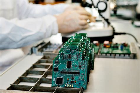
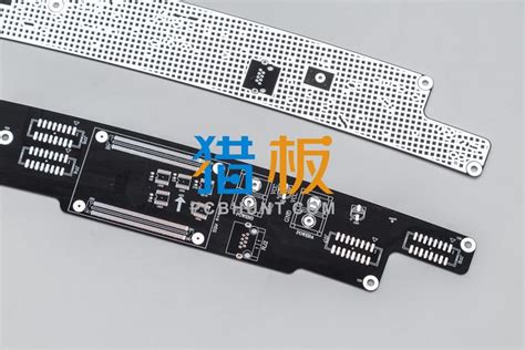
PCBA, short for Printed Circuit Board Assembly, represents a foundational stage in electronics manufacturing where components are mounted and interconnected on a PCB (Printed Circuit Board) to create functional circuits. At its core, PCB assembly transforms a bare board into an operational unit by integrating active and passive components such as resistors, capacitors, integrated circuits (ICs), and connectors. This process bridges design concepts with tangible hardware, enabling devices to perform tasks ranging from simple signal processing to complex computational operations.
A PCBA begins with a PCB, which serves as the physical platform for component placement. The board’s copper traces and layers are designed to route electrical signals, while solder pads and holes facilitate mechanical and electrical connections. During assembly, components are attached using techniques like surface-mount technology (SMT) or through-hole insertion, followed by soldering to secure them permanently. Critical to this stage is adherence to design specifications, thermal management, and signal integrity to ensure reliability and performance.
Understanding the distinction between PCB and PCBA is vital. While a PCB refers to the unpopulated board, a PCBA encompasses the fully assembled, tested, and functional product. This differentiation highlights the transformative role of PCB assembly in adding value to the base substrate. Modern PCBA processes rely on automated machinery for precision, minimizing human error and scaling production efficiently. Applications span industries—from consumer electronics and automotive systems to medical devices and industrial automation—underscoring its ubiquity in today’s technology-driven world.
By mastering the basics of PCBA, stakeholders can better navigate challenges in component sourcing, manufacturability, and quality assurance, ensuring robust outcomes in electronics development.
Key Components of a PCBA in Electronics Manufacturing
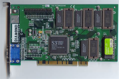
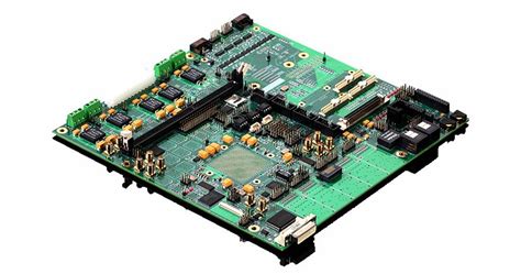
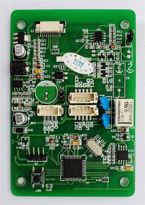
A PCBA (Printed Circuit Board Assembly) serves as the functional heart of most electronic devices, integrating critical hardware elements to enable seamless operation. At its core, a PCBA comprises several essential components, each playing a distinct role in ensuring performance and reliability. The printed circuit board (PCB) itself forms the structural foundation, providing mechanical support and electrical pathways through conductive copper traces. During PCB assembly, active and passive components are mounted onto the board. Active components, such as microcontrollers, transistors, and integrated circuits (ICs), process or amplify signals, while passive components like resistors, capacitors, and inductors manage voltage, current, and energy storage.
Connectors and interconnects, including headers, sockets, and terminal blocks, enable external device interfacing, ensuring compatibility with power supplies, sensors, or other subsystems. Solder, applied through techniques like reflow or wave soldering, secures these components to the PCB while establishing electrical continuity. Advanced PCBA designs may also incorporate surface-mount technology (SMT) components for compact layouts or through-hole components for enhanced mechanical stability in high-stress environments.
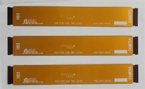
Material selection significantly impacts PCBA durability and functionality. For instance, substrates like FR-4 epoxy laminate balance cost and thermal resistance, while specialized ceramics or polyimide films cater to high-frequency or extreme-temperature applications. Additionally, thermal management elements—such as heat sinks or thermal pads—prevent overheating in power-intensive circuits, ensuring long-term reliability.
Quality in PCB assembly hinges on precise component placement, solder joint integrity, and adherence to design specifications. Automated optical inspection (AOI) and in-circuit testing (ICT) verify alignment, connectivity, and functionality, minimizing defects. By harmonizing these components, a well-executed PCBA delivers the performance, efficiency, and miniaturization demanded by modern electronics, from consumer gadgets to industrial automation systems.
The PCBA Manufacturing Process: Step-by-Step Overview
The PCBA (Printed Circuit Board Assembly) process is a systematic sequence of steps that transforms a bare PCB (Printed Circuit Board) into a functional electronic module. It begins with PCB fabrication, where the board’s base material, typically fiberglass or composite epoxy, is layered with conductive copper traces to create electrical pathways. Once the bare PCB is prepared, the pcb assembly phase commences. This involves applying solder paste to designated areas using a stencil, ensuring precise deposition for component placement.
Next, automated pick-and-place machines position surface-mount devices (SMDs) such as resistors, capacitors, and integrated circuits onto the board. These machines achieve micron-level accuracy, critical for modern high-density designs. The board then undergoes reflow soldering, where controlled heating melts the solder paste, forming permanent electrical connections. For through-hole components, wave soldering may be employed, immersing the board in a molten solder wave to secure leads.
After soldering, inspection and testing ensure quality. Automated Optical Inspection (AOI) systems scan for defects like misalignments or solder bridges, while X-ray inspection verifies hidden connections, such as those in Ball Grid Array (BGA) packages. Functional testing, including In-Circuit Testing (ICT) or boundary scan, validates electrical performance.
Finally, conformal coating may be applied to protect the PCBA from environmental factors like moisture or dust. The assembled board is then integrated into its final enclosure, completing the pcb assembly process. Each stage demands meticulous planning, as errors in component placement, soldering, or testing can compromise the entire assembly. By adhering to standardized workflows and leveraging advanced automation, manufacturers achieve the precision and reliability required for today’s complex electronic devices.
PCBA vs. PCB: Clarifying the Differences
Understanding the distinction between PCBA (Printed Circuit Board Assembly) and PCB (Printed Circuit Board) is critical in electronics manufacturing. A PCB refers to the bare, unpopulated board made of insulating material, such as fiberglass, with conductive copper traces etched onto its surface. It serves as the structural foundation for electronic components but lacks functionality until components are mounted. In contrast, PCBA represents the completed assembly, where components like resistors, capacitors, and integrated circuits are soldered onto the PCB through processes such as surface-mount technology (SMT) or through-hole assembly. This transformation from a passive board to an active circuit is the essence of PCB assembly.
The key difference lies in functionality: a PCB is inert, while a PCBA is operational. For example, a smartphone’s motherboard begins as a PCB, but only after undergoing PCB assembly—populating components, soldering, and testing—does it become a PCBA capable of processing signals. The term PCBA also emphasizes the integration of design, manufacturing, and testing phases, ensuring the final product meets performance standards.
Design complexity further differentiates the two. A PCB focuses on layout optimization to avoid signal interference, while PCBA demands precision in component placement, thermal management, and solder joint reliability. Missteps in PCB assembly can lead to defects like cold joints or short circuits, underscoring the importance of skilled execution.
In summary, PCB and PCBA represent sequential stages in electronics production: the former is the canvas, and the latter is the finished artwork. Recognizing this distinction ensures clarity in design, manufacturing, and troubleshooting workflows.
Design Considerations for Effective PCBA Development
Effective PCBA (Printed Circuit Board Assembly) development hinges on meticulous design strategies that balance functionality, manufacturability, and reliability. A well-optimized design ensures seamless integration of components during the PCB assembly process while minimizing errors and costs. Key considerations begin with component placement—arranging parts to avoid signal interference, reduce thermal stress, and simplify soldering. For instance, high-power components should be spaced apart to prevent overheating, while sensitive analog and digital circuits require isolation to mitigate electromagnetic interference (EMI).
Another critical factor is thermal management. Proper heat dissipation through strategic placement of thermal vias, heatsinks, or copper pours ensures the longevity of the PCBA in demanding environments. Designers must also account for trace routing to maintain signal integrity, especially in high-frequency applications. Differential pairs, controlled impedance traces, and minimized crosstalk are essential for preserving data accuracy.
Material selection plays a pivotal role in PCB assembly success. Choosing substrates with appropriate dielectric constants, thermal stability, and mechanical strength ensures compatibility with the intended application. Additionally, adhering to Design for Manufacturability (DFM) guidelines—such as standardizing component sizes, avoiding overly dense layouts, and providing adequate solder mask clearance—streamlines production and reduces defects.
Collaboration between design engineers and PCBA manufacturers is vital to address potential bottlenecks early. Prototyping and simulation tools, like finite element analysis (FEA), help validate designs before mass production. By prioritizing these elements, developers can achieve a robust, cost-effective PCBA that meets both performance and scalability demands.

Quality Control and Testing in PCBA Production
Ensuring reliability in PCB assembly (PCBA) requires rigorous quality control and testing protocols. These steps are critical to identifying defects, such as soldering inconsistencies, component misalignment, or electrical shorts, which could compromise the functionality of the final product. Automated Optical Inspection (AOI) systems are widely used to scan PCBA boards for visible flaws, while X-ray inspection detects hidden issues in solder joints, particularly in Ball Grid Array (BGA) components.
Functional testing validates the PCB assembly by simulating real-world operating conditions, ensuring all circuits and components perform as intended. In-circuit testing (ICT) checks individual component functionality, whereas environmental stress testing evaluates durability under extreme temperatures, humidity, or vibration. Advanced manufacturers also employ design-for-testability (DFT) principles during the PCBA design phase to streamline diagnostics and reduce failure risks.
Combining automated and manual inspections ensures comprehensive coverage, as human technicians can address nuanced defects that machines might overlook. By integrating these methodologies, manufacturers minimize rework costs, enhance yield rates, and deliver PCBA solutions that meet stringent industry standards for consumer electronics, automotive systems, and medical devices.
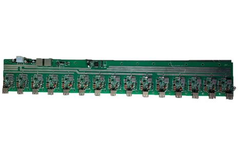
Applications of PCBA in Modern Electronic Devices
PCBA (Printed Circuit Board Assembly) serves as the backbone of countless modern electronic devices, enabling seamless integration of PCB assembly processes into industries that demand precision, reliability, and scalability. From consumer electronics to industrial machinery, PCBA technology powers devices by combining components like microcontrollers, sensors, and connectors into functional systems. In smartphones, for instance, compact PCBA designs allow for high-density layouts, ensuring advanced features such as 5G connectivity and AI-driven processing. Similarly, automotive systems rely on ruggedized PCB assemblies to withstand extreme temperatures and vibrations while managing critical functions like engine control and infotainment.
The healthcare sector benefits from PCBA through medical devices such as portable monitors and imaging equipment, where accuracy and compliance with safety standards are non-negotiable. Industrial automation leverages PCBA for programmable logic controllers (PLCs) and robotics, optimizing manufacturing efficiency through real-time data processing. Even everyday appliances like smart home devices utilize PCB assemblies to enable IoT connectivity, transforming homes into interconnected ecosystems.
Emerging fields like renewable energy and aerospace further highlight PCBA‘s versatility. Solar inverters and wind turbine controllers depend on robust PCB assemblies to manage power distribution, while satellites and drones use lightweight, high-performance PCBA designs for navigation and communication. The shift toward miniaturization and flexible circuits has also expanded applications in wearables, where ultra-thin PCB assemblies enable sleek, user-friendly designs.
As technology evolves, PCBA continues to adapt, addressing challenges like thermal management and signal integrity in high-frequency applications. Its role in enabling innovations—from edge computing to autonomous systems—underscores its irreplaceable position in modern electronics manufacturing.
Future Trends and Challenges in PCBA Technology
The evolution of PCB assembly (PCBA) technology continues to reshape electronics manufacturing, driven by demands for miniaturization, higher performance, and sustainability. A key trend is the adoption of high-density interconnect (HDI) designs, which enable compact yet powerful circuits critical for wearables, IoT devices, and advanced automotive systems. Additionally, advancements in automated optical inspection (AOI) and machine learning-driven quality control are enhancing precision in PCBA production, reducing defects and improving yield rates.
Sustainability is another focal point, with manufacturers prioritizing lead-free soldering, recyclable substrates, and energy-efficient processes to comply with global environmental regulations. However, these innovations come with challenges. The push for smaller components, such as 01005 passives or micro-BGA packages, demands ultra-precise placement equipment and rigorous thermal management strategies to prevent failures. Supply chain complexities, including shortages of specialized semiconductors, further complicate PCB assembly timelines and costs.
Tip: To address component scarcity, designers should collaborate early with suppliers to identify alternative parts and integrate modular designs that allow for flexibility in sourcing.
Looking ahead, the integration of PCBA with additive manufacturing (e.g., 3D-printed circuits) and hybrid rigid-flex boards could unlock new possibilities in custom electronics. Yet, ensuring signal integrity and durability in these emerging formats remains a hurdle. As the industry navigates these trends, balancing innovation with reliability will define the next era of electronics manufacturing.
Conclusion
In the rapidly evolving landscape of electronics manufacturing, understanding PCBA (Printed Circuit Board Assembly) remains fundamental to producing reliable and efficient electronic devices. The integration of components onto a PCB (Printed Circuit Board) through PCB assembly processes forms the backbone of modern electronics, enabling functionalities ranging from simple circuits to complex systems. As highlighted throughout this article, the distinction between PCBA and standalone PCBs lies in the former’s completed state, where components are mounted, soldered, and tested for operational readiness. Key considerations such as design precision, material selection, and automated assembly techniques directly influence the quality and performance of the final product. Quality control measures, including automated optical inspection (AOI) and functional testing, ensure that PCBA meets stringent industry standards, minimizing defects and enhancing longevity. Looking ahead, advancements in miniaturization, flexible electronics, and sustainability-driven practices will continue to shape PCB assembly methodologies, addressing challenges like component density and environmental compliance. By mastering these core concepts, manufacturers and engineers can navigate the complexities of PCBA development, driving innovation across industries such as consumer electronics, automotive systems, and IoT devices.
FAQs
What is the difference between a PCB and a PCBA?
A PCB (Printed Circuit Board) refers to the bare board without components, serving as the foundation for electrical connections. A PCBA (Printed Circuit Board Assembly) is the fully assembled board, incorporating all necessary electronic components like resistors, capacitors, and ICs. The PCB assembly process transforms a PCB into a functional PCBA.
What are the critical steps in the PCBA manufacturing process?
The PCBA process involves solder paste application, component placement (via pick-and-place machines), reflow soldering, inspection, and testing. Advanced techniques like Automated Optical Inspection (AOI) ensure quality, while functional testing validates performance.
Why is quality control vital in PCB assembly?
Defects in PCBA can lead to device failures, safety risks, or costly recalls. Rigorous quality control methods, such as X-ray inspection for hidden solder joints and environmental stress testing, ensure reliability and compliance with industry standards.
What industries rely heavily on PCBA technology?
PCBA is essential in consumer electronics, medical devices, automotive systems, and industrial automation. From smartphones to life-saving medical equipment, PCB assembly enables compact, high-performance electronic solutions.
How are modern PCBAs adapting to future technological demands?
Trends like miniaturization, high-speed signal integrity, and IoT integration drive innovations in PCBA design. Flexible circuits, advanced materials, and AI-driven assembly processes are reshaping the PCB assembly landscape.
What design considerations optimize PCBA performance?
Effective PCBA design prioritizes component placement, thermal management, and signal integrity. Tools like Design for Manufacturing (DFM) and simulation software help avoid assembly errors and enhance producibility.
Explore Professional PCB Assembly Solutions
For tailored PCBA services that meet industry standards, please click here to connect with experts in advanced PCB assembly and manufacturing.