PCBA Fault Rapid Diagnosis Guide
Introduction
Printed Circuit Board Assembly (PCBA) is a critical component in modern electronic devices. However, due to complex manufacturing processes, environmental factors, and operational stresses, PCBA faults are inevitable. Rapid diagnosis of these faults is essential to minimize downtime, reduce repair costs, and ensure product reliability.
This guide provides a structured approach to identifying and troubleshooting common PCBA faults efficiently.
1. Common PCBA Faults and Symptoms
Before diagnosing faults, it is crucial to recognize common failure modes and their symptoms:
1.1. Electrical Failures
- Short Circuits: Excessive current flow, overheating, or burnt components.
- Open Circuits: No continuity, non-functional circuits, or intermittent connections.
- Intermittent Connections: Random failures due to loose solder joints or cracked traces.
1.2. Soldering Defects
- Cold Solder Joints: Dull, cracked, or poorly bonded solder connections.
- Solder Bridges: Unintended connections between adjacent pads or pins.
- Insufficient Solder: Weak joints leading to intermittent failures.
1.3. Component Failures
- Failed ICs/Transistors: Overheating, no output signal, or incorrect voltage levels.
- Damaged Passive Components (Resistors, Capacitors): Discoloration, bulging, or incorrect readings.
- ESD (Electrostatic Discharge) Damage: Sudden failure without visible signs.
1.4. PCB-Related Issues
- Delamination: Blistering or separation of PCB layers.
- Trace Damage: Broken or corroded copper traces.
- Via Failures: Poor plating leading to open circuits.
1.5. Environmental & Mechanical Damage
- Moisture Ingress: Corrosion, leakage currents, or short circuits.
- Physical Stress: Cracked PCBs or broken components due to impact.
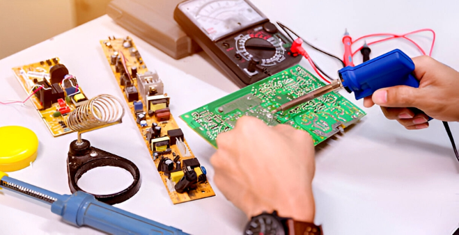
2. Tools for Rapid PCBA Fault Diagnosis
To efficiently diagnose PCBA faults, the following tools are essential:
- Multimeter: Measures voltage, resistance, and continuity.
- Oscilloscope: Analyzes signal integrity and waveform distortions.
- Thermal Camera: Detects overheating components.
- Microscope/Magnifying Lens: Inspects solder joints and tiny components.
- Automated Optical Inspection (AOI): Automated detection of soldering defects.
- In-Circuit Tester (ICT): Validates component functionality.
- X-Ray Inspection: Detects hidden defects like BGA (Ball Grid Array) solder issues.
3. Step-by-Step PCBA Fault Diagnosis Process
3.1. Visual Inspection
- Check for burnt components, discolored areas, or bulging capacitors.
- Examine solder joints for cracks, bridges, or insufficient solder.
- Look for physical damage (cracks, bent pins, or broken traces).
3.2. Power-On Testing
- Apply power and check for smoke, overheating, or abnormal sounds.
- Measure input voltage to ensure correct power supply.
- Use a thermal camera to identify hotspots.
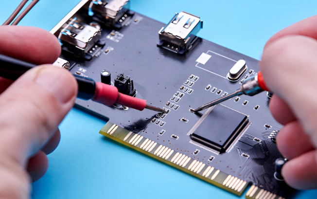
3.3. Continuity & Resistance Checks
- Use a multimeter in continuity mode to detect open/short circuits.
- Measure resistance across critical traces to identify high-resistance faults.
3.4. Signal Tracing & Oscilloscope Analysis
- Probe key test points to verify signal integrity.
- Compare waveforms with reference designs to detect anomalies.
- Check clock signals, data lines, and power rails for noise or distortion.
3.5. Component-Level Testing
- Test diodes, transistors, and ICs for proper functionality.
- Replace suspected faulty components and retest.
3.6. Environmental Stress Testing (If Needed)
- Perform thermal cycling to detect intermittent faults.
- Use vibration testing to identify loose connections.
4. Advanced Diagnostic Techniques
4.1. Boundary Scan Testing (JTAG)
- Used for digital ICs to verify interconnections and logic states.
4.2. Flying Probe Testing
- Automated testing for unpopulated or prototype PCBAs.
4.3. Functional Testing (FCT)
- Validates the entire PCBA functionality under real operating conditions.
4.4. Machine Learning-Based Fault Detection
- AI-powered systems analyze historical failure data to predict and diagnose faults faster.
5. Preventive Measures to Reduce PCBA Failures
- Proper Soldering Techniques: Use reflow/selective soldering for consistency.
- ESD Protection: Ground workstations and use anti-static mats.
- Conformal Coating: Protects against moisture and dust.
- Regular Testing: Implement AOI, ICT, and functional tests during production.
- Design for Testability (DFT): Include test points for easier diagnostics.
6. Conclusion
Rapid PCBA fault diagnosis requires a systematic approach, combining visual inspection, electrical testing, signal analysis, and advanced diagnostic tools. By understanding common failure modes and leveraging the right techniques, engineers can minimize downtime and improve repair efficiency.
Implementing preventive measures and automated testing further enhances PCBA reliability, ensuring long-term performance in electronic systems.


