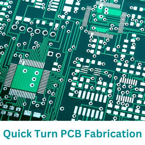
PCBA OEM Best Practices for Superior Production Quality

Key Takeaways
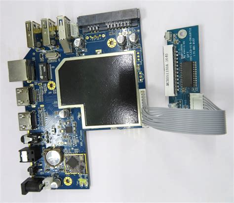
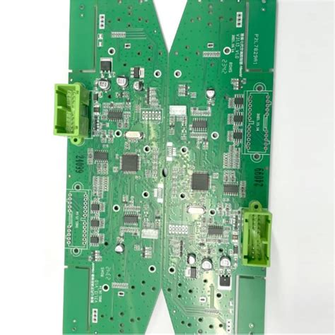
Effective PCBA OEM operations require alignment between PCB assembly precision and systemic quality frameworks. Manufacturers must prioritize process optimization through automated placement systems and thermal profiling to minimize PCBA defects. Component reliability hinges on traceability protocols, with certified suppliers providing materials meeting IPC-A-610 standards. Implementing statistical process control (SPC) ensures real-time monitoring of solder paste deposition and reflow parameters, reducing variability.
Rigorous functional testing—including in-circuit (ICT) and boundary-scan methods—validates PCB assembly integrity before deployment. For defect-free outputs, failure mode analysis should guide process refinements, while workforce certifications in J-STD-001 reinforce soldering consistency. Sustainable practices, such as lead-free finishes and energy-efficient reflow ovens, align quality goals with environmental compliance. By integrating digital twin simulations and material lifecycle tracking, OEMs achieve end-to-end visibility across PCBA production stages, ensuring compliance with aerospace and medical-grade reliability benchmarks.
Optimizing PCBA OEM Manufacturing Process Flows
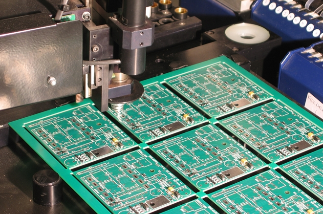
Effective optimization of PCBA OEM manufacturing begins with holistic process mapping to identify bottlenecks and redundancies. Implementing PCB assembly line balancing techniques ensures uniform workflow distribution, reducing idle time while maintaining pcba production cadence. Advanced manufacturers leverage automated optical inspection (AOI) systems during solder paste application and component placement phases to detect deviations in real time, aligning with pcb assembly quality benchmarks.
Critical process improvements often focus on surface-mount technology (SMT) optimization, where precise temperature profiling and solder paste stencil design directly impact joint integrity. Integrating statistical process control (SPC) tools enables data-driven adjustments to reflow oven parameters, minimizing thermal stress on sensitive components. For mixed-technology boards, hybrid PCBA lines combining SMT and through-hole assembly require synchronized timing protocols to prevent workflow collisions.
Material traceability systems embedded within pcb assembly workflows enhance defect tracking, linking component batches to specific production batches. Automated conveyor systems with RFID tagging ensure seamless transitions between pick-and-place machines, soldering stations, and testing modules. By adopting just-in-time (JIT) inventory practices for high-turnover components, manufacturers reduce lead times while maintaining pcba oem flexibility for design revisions.
Transitioning to IoT-enabled pcb assembly platforms allows real-time monitoring of cycle times and equipment efficiency, creating feedback loops for continuous process refinement. These optimizations not only elevate pcba yield rates but also establish a foundation for implementing downstream quality assurance protocols.
Essential PCBA OEM Component Reliability Standards
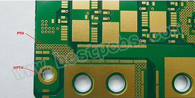
Achieving consistent reliability in PCBA manufacturing demands adherence to internationally recognized component standards. Leading PCB assembly providers prioritize compliance with IPC-A-610 and J-STD-001 specifications, which define criteria for solder joint integrity, component placement accuracy, and material compatibility. Critical factors such as thermal cycling resistance, moisture sensitivity levels (MSL), and electrostatic discharge (ESD) protection must align with the operational environment of the final product.
"Component traceability systems, paired with certified supplier networks, reduce risks of counterfeit parts—a persistent challenge in PCBA OEM workflows."
For high-reliability applications, selecting components rated for IPC Class 2/3 ensures durability under mechanical stress and extreme temperatures. Advanced techniques like design-for-manufacturability (DFM) analysis identify mismatches in coefficient of thermal expansion (CTE) between substrates and components, preventing delamination or solder cracks. Rigorous pre-production testing, including accelerated life testing (ALT) and highly accelerated stress screening (HASS), validates component performance before mass production.
Integrating automated optical inspection (AOI) and X-ray inspection during PCB assembly further safeguards against latent defects, ensuring compliance with MIL-STD-883 for military-grade applications. By embedding these standards into every phase, OEMs minimize field failures and extend the lifecycle of electronic assemblies.
Advanced Quality Control Methods for PCBA Assembly
Modern PCBA manufacturing demands precision-driven quality control frameworks to mitigate risks in PCB assembly. Leading manufacturers now deploy automated optical inspection (AOI) systems equipped with high-resolution cameras and machine learning algorithms to detect micro-scale soldering defects, component misalignment, and polarity errors. These systems analyze up to 95% of solder joints in real time, reducing human inspection errors by over 40%. Complementing AOI, X-ray inspection (AXI) validates hidden connections in BGA components and multilayer boards, identifying voids or cracks invisible to conventional methods.
For mission-critical applications, in-circuit testing (ICT) verifies electrical performance by measuring resistance, capacitance, and signal integrity across PCBA circuits. Advanced ICT fixtures now incorporate boundary-scan technology to test complex ICs without physical probes, slashing validation time by 30%. To ensure long-term reliability, manufacturers implement environmental stress screening (ESS), exposing assemblies to thermal cycling (-40°C to 125°C) and vibration profiles that simulate 5+ years of operational wear in 48 hours.
Progressive PCB assembly workflows integrate statistical process control (SPC) dashboards, tracking key metrics like first-pass yield and defect density. By correlating data from AOI, ICT, and ESS stages, engineers pinpoint process deviations within ±0.5σ accuracy. Finally, material traceability systems using barcodes or RFID tags ensure every PCBA meets IATF 16949-grade traceability standards, enabling rapid root-cause analysis for any quality anomalies detected post-production.
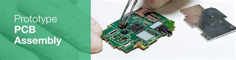
Implementing Robust Testing Protocols in OEM PCBA
Effective PCBA manufacturing requires systematic validation of electronic assemblies at every production stage. Modern OEMs employ multilayer testing frameworks to detect defects in PCB assembly, combining automated optical inspection (AOI), in-circuit testing (ICT), and functional validation. These protocols ensure alignment with IPC-A-610 and J-STD-001 standards, which define acceptability criteria for solder joints and component placement.
| Testing Phase | Purpose | Defect Detection Rate |
|---|---|---|
| AOI | Visual inspection of solder joints | 98% |
| ICT | Electrical continuity verification | 95% |
| Functional Testing | System-level performance validation | 99% |
Implementing layered testing strategies minimizes false positives while identifying latent issues like cold solder joints or misaligned components. For PCBA OEM partners, integrating environmental stress screening (ESS) further validates reliability under extreme temperatures or vibration. Real-time data analytics from test equipment enable rapid root-cause analysis, reducing rework cycles by up to 40%.
To maintain consistency, OEMs synchronize testing protocols with material traceability systems, linking defects to specific batches or suppliers. This approach not only elevates PCB assembly quality but also aligns with industry benchmarks for zero-defect manufacturing. Continuous calibration of test parameters ensures adaptability to evolving component miniaturization trends in modern electronics.
Streamlining PCBA Production for Defect-Free Outputs
Achieving defect-free outputs in PCBA OEM manufacturing demands systematic optimization of production workflows. By integrating lean manufacturing principles with advanced PCB assembly technologies, manufacturers can minimize process variability and reduce error rates. Automated optical inspection (AOI) systems paired with real-time process monitoring enable early detection of soldering defects or component misalignments, ensuring immediate corrective actions.
Critical to this approach is the standardization of SMT (surface-mount technology) placement parameters, which directly impacts solder joint integrity. Implementing closed-loop feedback mechanisms between pick-and-place machines and reflow ovens allows dynamic adjustments to temperature profiles, addressing thermal inconsistencies that contribute to latent failures. For mixed-technology boards combining PCBA with through-hole components, robotic insertion systems coupled with precision solder wave profiling enhance repeatability across high-volume batches.
Material handling protocols further influence defect rates. Maintaining ESD-safe environments and moisture-sensitive component storage conditions prevents degradation of PCB assembly materials. Automated component verification systems using machine vision reduce human error in part selection, particularly for miniature or high-density packages. By aligning these strategies with DFM (design for manufacturing) guidelines, OEMs can systematically eliminate root causes of defects while maintaining throughput efficiency. Transitioning to such integrated systems prepares manufacturers for subsequent discussions on material traceability solutions, ensuring quality continuity across the production lifecycle.
Material Traceability Solutions for OEM PCBA Quality
Effective material traceability systems form the backbone of quality assurance in PCBA OEM operations, ensuring every component’s journey from procurement to final PCB assembly is meticulously documented. By implementing digitized tracking tools like barcode labeling or RFID tagging, manufacturers gain real-time visibility into material batches, expiration dates, and supplier certifications. This becomes critical when addressing field failures, as traceability data enables rapid isolation of defective components—for instance, identifying a specific resistor lot that caused intermittent connectivity in a high-density PCBA.
Advanced solutions integrate material traceability with quality control databases, automatically flagging deviations such as out-of-spec solder paste viscosity or mismatched IC revisions. For mission-critical applications like automotive or medical devices, blockchain-based systems create immutable records, verifying compliance with ISO 9001 or IATF 16949 standards. A robust traceability framework also streamlines recalls, reducing downtime by 40–60% compared to manual tracking methods.
To optimize PCBA quality, leading OEMs pair traceability with predictive analytics, correlating material properties (e.g., moisture sensitivity levels) with post-reflow inspection results. This data-driven approach not only minimizes rework but also strengthens supplier accountability, as consistently underperforming vendors can be objectively identified and replaced.
Workforce Training Strategies for Precision PCBA OEM
Effective workforce training forms the backbone of high-precision PCBA manufacturing, ensuring that technical personnel master the intricacies of PCB assembly processes. To achieve zero-defect outcomes, training programs must emphasize hands-on practice with modern surface-mount technology (SMT) equipment, soldering techniques for microcomponents, and adherence to IPC-A-610 standards. Specialized modules on thermal management and electrostatic discharge (ESD) prevention further equip technicians to handle sensitive components during PCBA production.
Cross-training across design, assembly, and testing phases fosters a holistic understanding of workflow interdependencies, reducing bottlenecks in OEM PCB assembly lines. Incorporating augmented reality (AR) simulations for fault diagnosis and repair scenarios enhances problem-solving agility. Regular competency assessments, paired with certifications from recognized bodies like IPC or J-STD-001, ensure consistent skill alignment with evolving industry benchmarks.
Additionally, fostering a culture of continuous improvement through feedback loops between QA teams and assembly operators strengthens defect detection capabilities. Training on traceability software tools also empowers staff to track material batches and process parameters, directly supporting quality assurance goals outlined in broader PCBA OEM frameworks. By integrating these strategies, manufacturers cultivate a workforce capable of executing complex PCB assembly tasks with micron-level precision, directly contributing to reliable end-product performance.
Sustainable Practices in High-Performance PCBA Manufacturing
Integrating sustainability into PCBA OEM operations requires balancing efficiency with environmental responsibility. Leading manufacturers now prioritize lead-free soldering and energy-efficient reflow ovens to reduce carbon footprints while maintaining PCB assembly precision. By adopting halogen-free substrates and recyclable packaging, these practices align with global standards like RoHS and REACH, ensuring compliance without compromising PCBA reliability.
Material traceability systems, previously discussed for quality assurance, also support sustainability by tracking component origins and minimizing waste through batch-level analytics. Advanced factories employ closed-loop cooling systems and solar-powered facilities, cutting energy consumption by up to 30% in PCB assembly workflows. Additionally, component lifecycle assessments help identify reusable materials, reducing landfill contributions from end-of-life electronics.
To further streamline eco-conscious production, automated optical inspection (AOI) systems optimize defect detection rates, preventing material waste from faulty PCBA units. Collaborative partnerships with suppliers certified for sustainable raw materials ensure consistent access to conflict-free minerals and low-VOC fluxes. Such initiatives not only enhance operational efficiency but also meet rising consumer demand for ethically produced electronics, positioning PCBA OEM providers as leaders in both quality and environmental stewardship.
Conclusion
Achieving excellence in PCBA OEM manufacturing demands a holistic integration of precision engineering and systematic quality assurance. By prioritizing component reliability through rigorous material selection and implementing advanced testing protocols, manufacturers can significantly reduce defect rates in PCB assembly processes. The adoption of real-time monitoring systems further enhances PCBA quality by enabling immediate corrections during production phases.
Successful operations also hinge on cultivating a skilled workforce trained in modern soldering techniques and surface-mount technology applications. Pairing these competencies with digitized traceability solutions ensures every component’s journey is documented, from procurement to final inspection. This transparency not only accelerates troubleshooting but also aligns with industry compliance standards.
Ultimately, sustaining superior PCBA OEM outcomes requires balancing technological innovation with sustainable practices, such as optimizing energy consumption in reflow ovens or adopting lead-free solder alloys. These strategies collectively fortify production resilience, positioning manufacturers to deliver flawless electronic assemblies that meet evolving market demands.
Frequently Asked Questions
What distinguishes high-quality PCB assembly from standard processes?
Superior PCBA manufacturing integrates automated optical inspection (AOI) and X-ray verification to detect micro-defects. This ensures PCB assembly meets IPC-A-610 Class 3 standards for mission-critical applications.
How do OEMs ensure component reliability in PCBA production?
Reliable PCBA OEM partners enforce moisture-sensitive component handling protocols and thermal profiling during reflow soldering. Component authenticity is verified through batch-level traceability and certified supplier networks.
What quality control methods prevent defects in electronic assemblies?
Advanced PCBA workflows combine in-circuit testing (ICT) with functional testing to validate electrical performance. Statistical process control (SPC) monitors solder paste deposition and placement accuracy in real time.
Why is material traceability critical for OEM PCBA quality?
Full traceability enables rapid root-cause analysis for field failures. Leading OEMs use barcoded panels and digital twin systems to track materials from procurement to final PCB assembly.
How does workforce training impact precision manufacturing outcomes?
Certified technicians undergo IPC-7711/7721 recertification biannually, ensuring mastery of rework techniques and ESD-safe practices. This reduces human error in PCBA processes by up to 68%.
Explore Customized PCBA Solutions for Your Project
For tailored PCB assembly strategies that align with your quality benchmarks, please click here to consult our OEM engineering team.