Photonic Printed Circuit Boards (PCBs): The Future of High-Speed Data Transmission
Introduction
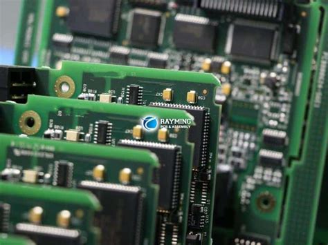
The rapid advancement of computing, telecommunications, and data centers has led to an increasing demand for faster and more efficient data transmission technologies. Traditional electronic printed circuit boards (PCBs) rely on copper traces to transmit electrical signals, but they face limitations such as signal attenuation, electromagnetic interference (EMI), and power consumption at high frequencies. To overcome these challenges, photonic PCBs—which use light instead of electricity for data transmission—have emerged as a revolutionary alternative.
Photonic PCBs integrate optical waveguides, lasers, modulators, and photodetectors into conventional PCB substrates, enabling ultra-high-speed data transfer with minimal losses. This article explores the principles, advantages, manufacturing techniques, applications, and future prospects of photonic PCBs.
1. Principles of Photonic PCBs
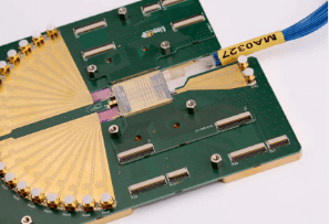
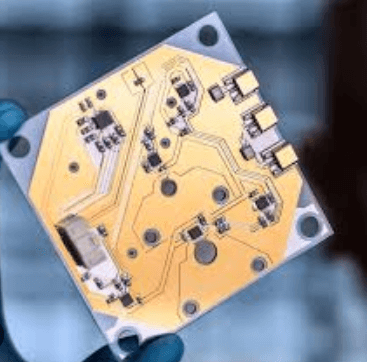
Photonic PCBs leverage optical interconnects to transmit data as light pulses through waveguides made of dielectric materials such as silicon nitride (SiN) or polymers. The key components include:
- Optical Waveguides: Thin, transparent structures that guide light signals similarly to how copper traces guide electrical signals.
- Light Sources: Typically laser diodes or vertical-cavity surface-emitting lasers (VCSELs) that generate optical signals.
- Modulators: Devices that encode electrical data onto optical carriers (e.g., Mach-Zehnder modulators).
- Photodetectors: Convert optical signals back into electrical signals (e.g., germanium or InGaAs-based detectors).
- Couplers & Splitters: Direct and distribute optical signals efficiently.
Unlike electrical signals, optical signals do not suffer from resistive losses or EMI, allowing for higher bandwidth and longer transmission distances without signal degradation.
2. Advantages of Photonic PCBs
2.1 Higher Bandwidth & Speed
Optical signals can carry data at terabit-per-second (Tbps) speeds, far exceeding the capabilities of copper interconnects, which are limited by skin effect and crosstalk at high frequencies.
2.2 Lower Power Consumption
Electrical interconnects require significant power to maintain signal integrity over distance, whereas photonic interconnects consume less energy, reducing heat generation and improving energy efficiency.
2.3 Reduced Electromagnetic Interference (EMI)
Since light does not generate electromagnetic fields, photonic PCBs eliminate EMI issues, making them ideal for high-frequency applications like 5G/6G, radar, and aerospace systems.
2.4 Lower Latency
Light travels faster than electrons in copper, reducing propagation delays—a critical factor in high-performance computing (HPC) and artificial intelligence (AI) applications.
2.5 Scalability & Miniaturization
Photonic waveguides can be fabricated at micrometer scales, allowing for denser interconnects and more compact PCB designs compared to bulky copper traces.
3. Manufacturing Techniques for Photonic PCBs
3.1 Waveguide Fabrication
- Laser Direct Writing: Uses ultrafast lasers to pattern waveguides in glass or polymer substrates.
- Photolithography & Etching: Similar to semiconductor manufacturing, where waveguides are defined using UV exposure and chemical etching.
- 3D Printing: Emerging additive manufacturing techniques enable flexible waveguide integration.
3.2 Hybrid Integration
Combining electronic and photonic components requires:
- Flip-Chip Bonding: Attaching laser diodes and photodetectors directly onto the PCB.
- Through-Silicon Vias (TSVs): Enabling vertical optical connections in multilayer PCBs.
3.3 Materials
- Silicon Photonics: Silicon-on-insulator (SOI) platforms for high-performance applications.
- Polymer Waveguides: Cost-effective and flexible for consumer electronics.
- Glass Substrates: Ultra-low-loss waveguides for long-distance communication.
4. Applications of Photonic PCBs
4.1 Data Centers & Cloud Computing
Photonic interconnects reduce bottlenecks in server-to-server communication, improving efficiency in hyperscale data centers.
4.2 Telecommunications & 5G/6G Networks
High-speed optical backplanes enable faster fiber-optic and wireless communication infrastructures.
4.3 High-Performance Computing (HPC) & AI
Low-latency photonic interconnects accelerate data transfer in supercomputers and AI accelerators.
4.4 Automotive & Aerospace
EMI-free optical links enhance reliability in autonomous vehicles, avionics, and satellite communications.
4.5 Medical Imaging & Sensing
Photonic PCBs enable compact, high-resolution optical sensors for biomedical applications.
5. Challenges & Future Prospects
Despite their advantages, photonic PCBs face several challenges:
- High Manufacturing Costs: Precision fabrication techniques are still expensive.
- Thermal Management: Lasers and photonic components generate localized heat.
- Standardization: Lack of uniform design rules for optical PCB integration.
However, ongoing research in silicon photonics, plasmonics, and quantum photonics promises to overcome these hurdles. Future developments may include:
- Fully Optical Computing: Eliminating electronic components entirely.
- Quantum Photonic PCBs: Enabling ultra-secure quantum communication.
- Self-Healing Waveguides: Materials that repair optical pathways automatically.
Conclusion
Photonic PCBs represent a transformative shift in high-speed data transmission, offering unparalleled bandwidth, energy efficiency, and reliability compared to traditional electronic PCBs. While challenges remain in cost and integration, advancements in fabrication and materials science are accelerating their adoption across industries. As the demand for faster, more efficient computing grows, photonic PCBs are poised to become the backbone of next-generation communication and processing systems, ushering in a new era of optical electronics.