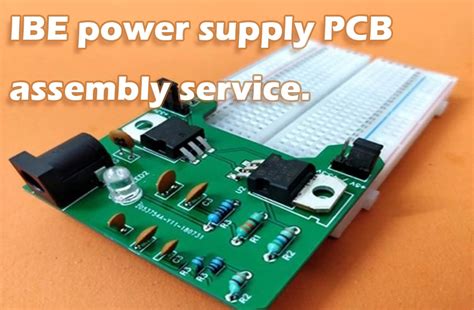
Power Supply PCB Assembly Design Strategies for Robust Performance
Key Takeaways
Effective PCB assembly for power supplies demands a holistic approach that balances thermal, electrical, and regulatory considerations. Below are the core principles to ensure robust performance in high-current and high-voltage applications:
- Thermal management is non-negotiable. Use copper pours, thermal vias, and heatsinks to dissipate heat efficiently.
- Optimize component placement to minimize trace lengths and reduce parasitic inductance, critical for stable power delivery.
- EMI reduction requires strategic shielding, proper grounding, and decoupling capacitors near noise-sensitive components.
- Adherence to compliance standards (e.g., IPC-2221, UL 60950) ensures safety and reliability in PCBA designs.
"Integrating thermal and electrical design early in the PCB assembly process prevents costly redesigns and enhances longevity," notes a senior power electronics engineer.
| Design Priority | Implementation Strategy |
|---|---|
| Heat Dissipation | Use 2 oz copper layers for high-current paths |
| Signal Integrity | Route high-frequency traces away from analog circuits |
| Regulatory Compliance | Validate spacing and isolation per IEC 62368-1 |
Pro Tip: Always prototype PCBA layouts with thermal imaging to identify hotspots before mass production. This step ensures compliance and performance under real-world conditions.
By aligning material selection (e.g., FR-4 with high Tg) with operational demands, designers can achieve high-efficiency power supply PCB assemblies that meet both technical and regulatory benchmarks.
Power Supply PCB Thermal Management Strategies
Effective thermal management in PCB assembly is critical for maintaining the reliability and longevity of power supply systems. High-current components, such as MOSFETs and voltage regulators, generate significant heat, which, if unmanaged, can degrade performance or cause premature failure. A foundational strategy involves optimizing copper pour layouts to distribute heat evenly across the board. Thick copper layers (2 oz or higher) enhance current-carrying capacity while acting as natural heat spreaders.
Strategic placement of thermal vias beneath heat-generating components facilitates heat transfer to inner ground planes or dedicated thermal pads. For PCBA designs operating in demanding environments, integrating active cooling solutions—like heatsinks or fans—complements passive techniques. Designers should prioritize component spacing to prevent thermal coupling, ensuring hot spots do not affect adjacent sensitive circuits.
Material selection also plays a pivotal role. High-temperature substrates, such as polyimide or ceramic-filled laminates, offer superior thermal stability compared to standard FR4. Additionally, using thermal interface materials (TIMs) between components and heatsinks minimizes thermal resistance.
Simulation tools, such as finite element analysis (FEA), enable precise modeling of heat distribution during the PCB assembly phase, allowing iterative improvements before prototyping. Balancing thermal performance with electromagnetic compatibility (EMC) and power integrity remains essential, as excessive copper for heat dissipation may inadvertently increase parasitic inductance. By aligning thermal strategies with broader PCBA design goals, engineers achieve robust, high-efficiency power systems capable of meeting stringent industry standards.
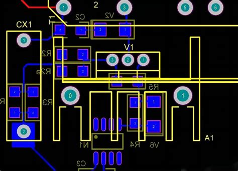
Optimizing Component Placement for Efficient Power Delivery
Effective PCB assembly for power supply systems demands strategic component placement to minimize energy loss and maximize operational stability. High-current paths should be prioritized, with power transistors, inductors, and capacitors positioned to shorten trace lengths, reducing resistive losses and voltage drops. Placing heat-sensitive components like MOSFETs away from high-temperature areas ensures thermal reliability, while grouping analog control circuits separately from noisy digital sections prevents signal interference.
In PCBA layouts, the orientation of magnetic components (e.g., transformers) must align with electromagnetic field directions to avoid coupling issues. Decoupling capacitors should be placed as close as possible to IC power pins to suppress voltage fluctuations, and ground planes must be strategically partitioned to isolate sensitive circuitry. Additionally, maintaining adequate spacing between high-voltage traces and low-voltage control lines minimizes parasitic capacitance risks.
A modular approach to component grouping—organizing functional blocks (rectification, filtering, regulation) into distinct zones—streamlines both design and troubleshooting. This method also enhances manufacturability by simplifying soldering processes during PCB assembly. By balancing electrical performance with thermal and mechanical constraints, engineers can achieve power delivery systems that meet efficiency benchmarks while adhering to industry-standard reliability requirements.
EMI Reduction Techniques in Power Supply PCB Design
Effective PCB assembly for power supplies demands meticulous attention to electromagnetic interference (EMI) mitigation, as uncontrolled noise can degrade performance and violate regulatory standards. A foundational strategy involves optimizing grounding schemes, such as employing star grounding or dedicated ground planes, to minimize loop areas and prevent parasitic currents. In PCBA layouts, segregating high-frequency switching components (e.g., MOSFETs, diodes) from sensitive analog circuits through strategic zoning reduces inductive coupling.
Another critical aspect is the use of shielding techniques, including ferrite beads or shielded inductors, to contain high-frequency emissions. Proper decoupling capacitor placement near power pins and the integration of EMI filters (π-filters, common-mode chokes) further suppress noise propagation. For multilayer designs, placing power and ground layers adjacent to signal layers enhances impedance control and minimizes radiated interference.
Additionally, trace routing practices—such as avoiding 90° angles and maintaining adequate spacing between high-current paths—help mitigate crosstalk. Compliance with standards like CISPR 32 or FCC Part 15 often necessitates post-assembly EMI testing, underscoring the importance of iterative prototyping in PCB assembly workflows. By harmonizing these techniques, engineers achieve robust EMI performance without compromising power delivery efficiency in PCBA systems.
Compliance Standards for Reliable PCB Power Assemblies
Adhering to industry compliance standards is non-negotiable for ensuring the safety, reliability, and longevity of power supply PCB assemblies. Regulatory frameworks such as IPC-2221 for design guidelines, UL 60950-1 for safety certifications, and IEC 62368-1 for hazard-based engineering define critical benchmarks for PCBA development. These standards address thermal thresholds, electrical isolation, and material flammability ratings, ensuring assemblies operate safely under high-load conditions.
Designers must integrate compliance checks early in the PCB assembly process, particularly for trace spacing and creepage distances, to prevent arcing or short circuits. For global markets, RoHS and REACH directives mandate strict limits on hazardous substances, influencing both component selection and soldering techniques. Rigorous testing protocols—including thermal cycling and high-potential (hipot) testing—validate adherence to these requirements before mass production.
Transitioning from design to manufacturing, collaboration with certified PCBA partners ensures alignment with ISO 9001 quality management systems. Documentation of compliance, such as test reports and material declarations, becomes essential for audits and certifications. By embedding these standards into every phase, engineers mitigate risks while delivering power supply PCB assemblies that meet global performance and safety expectations.
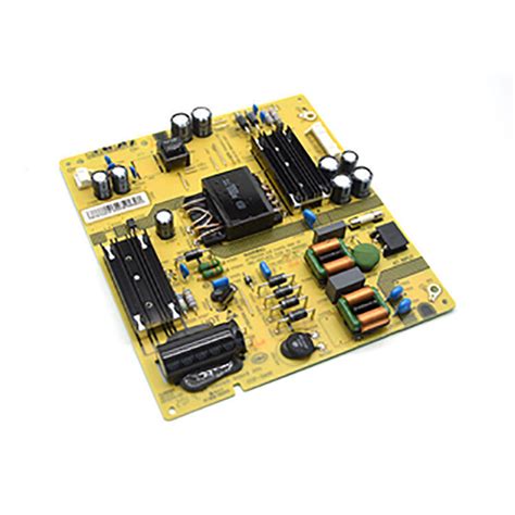
Enhancing Performance Through Robust PCB Layout Design
Effective PCB assembly relies heavily on intelligent layout design to balance electrical performance, thermal efficiency, and manufacturability. A well-structured PCBA layout begins with optimizing trace routing to minimize resistance and voltage drops, particularly in high-current paths. Critical components such as power MOSFETs, transformers, and filter capacitors require strategic placement to reduce parasitic inductance and ensure stable power delivery. For instance, positioning decoupling capacitors close to IC power pins mitigates high-frequency noise, while maintaining adequate spacing between heat-generating components prevents localized thermal buildup.
Layer stackup configuration plays a pivotal role in PCB assembly success. A dedicated power plane minimizes impedance and enhances current distribution, whereas a solid ground plane shields sensitive circuits from electromagnetic interference (EMI). Implementing star-point grounding for analog and digital sections avoids ground loops, preserving signal integrity. Advanced PCBA designs often incorporate thermal vias beneath high-power devices to channel heat toward inner layers or heatsinks, aligning with broader thermal management strategies.
Transitioning to manufacturing considerations, adherence to DFM (Design for Manufacturing) principles ensures reliable PCB assembly outcomes. This includes adhering to clearance rules for high-voltage traces and verifying solder mask openings for precise component soldering. Simulation tools like SPICE or finite element analysis (FEA) can validate layout choices before prototyping, reducing iteration cycles. By harmonizing electrical, thermal, and mechanical requirements, robust PCB layouts form the backbone of high-performance power supply systems, directly influencing long-term reliability and compliance with industry standards.
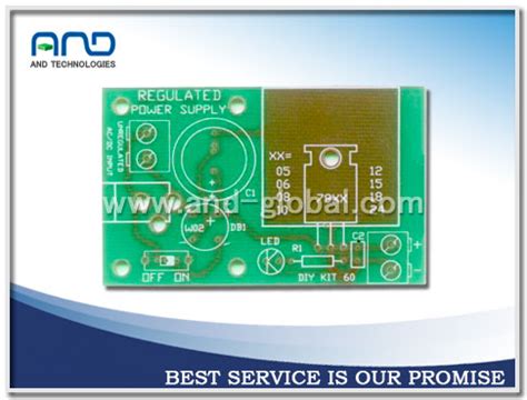
Material Selection Criteria for Durable Power Supply PCBs
Selecting appropriate materials is foundational to ensuring the longevity and reliability of power supply PCB assemblies. The substrate material’s thermal stability and dielectric properties directly influence performance, particularly in high-current applications. For instance, PCBA designs often prioritize materials like FR-4 with high glass transition temperatures (Tg) to withstand elevated operating temperatures, minimizing warping or delamination. In scenarios requiring enhanced thermal dissipation, metal-core substrates or ceramics may be integrated to improve heat transfer away from critical components.
Copper weight and trace thickness also play pivotal roles, as thicker copper layers reduce resistive losses and improve current-carrying capacity. Additionally, dielectric materials with low dissipation factors help mitigate signal integrity issues in high-frequency PCB assembly applications. Compliance with industry standards such as IPC-4101 ensures material consistency, while flame-retardant laminates (e.g., UL 94 V-0 rated) address safety requirements.
For PCBA longevity, consider environmental factors like humidity resistance. Materials with low moisture absorption rates, such as polyimide or PTFE-based substrates, prevent degradation in harsh conditions. Balancing cost and performance is critical—premium materials may elevate initial expenses but reduce failure risks over the product lifecycle. By aligning material choices with operational demands, engineers can optimize both durability and functionality in power supply PCB assemblies.
Integrating Thermal and Electrical Design in PCB Assemblies
Effective PCB assembly for power supplies demands synergistic integration of thermal and electrical design principles. Thermal vias, strategically placed copper pours, and heatsink integration must align with high-current pathways to prevent localized heating from degrading component performance. This approach ensures that heat-generating elements like MOSFETs or voltage regulators maintain optimal operating temperatures while preserving signal integrity across the PCBA.
Critical considerations include positioning high-power components to minimize conductive thermal transfer to sensitive analog circuits. Routing power traces with adequate width and spacing reduces resistive losses, while maintaining proper clearance between high-voltage nodes prevents arcing risks. Simultaneously, implementing thermal relief patterns in ground planes balances heat dissipation with electrical connectivity requirements.
Material selection further bridges thermal and electrical needs. Using substrates with high thermal conductivity, such as metal-core or ceramic-filled laminates, enhances heat distribution without compromising dielectric strength. Advanced simulation tools enable designers to model electrothermal interactions, predicting hotspots before prototyping. For PCB assembly reliability, adhering to IPC-2221 thermal management guidelines and IPC-9592 power conversion standards ensures designs meet both electrical specifications and thermal endurance thresholds.
Best Practices for High-Efficiency Power Supply PCB Assembly
Achieving high efficiency in PCB assembly for power supplies requires meticulous attention to both electrical and thermal dynamics. Start by optimizing component placement to minimize parasitic inductance and resistance in high-current paths. Place power semiconductors, transformers, and filtering capacitors in proximity to reduce loop areas, which directly impacts electromagnetic interference (EMI) and energy loss. Implement thermal vias beneath heat-generating components like MOSFETs or voltage regulators to enhance heat dissipation, pairing them with copper pours or heatsinks for effective thermal management.
When designing PCBA layouts, prioritize low-impedance power planes and ensure proper isolation between analog and digital sections to prevent noise coupling. Utilize star routing for critical traces to avoid ground loops and maintain signal integrity. For high-frequency switching circuits, maintain consistent trace widths and avoid sharp angles to mitigate impedance mismatches. Material selection also plays a pivotal role—opt for substrates with high glass transition temperatures (Tg) and low dielectric losses to withstand thermal cycling and improve reliability.
Finally, validate designs through iterative prototyping and rigorous testing, focusing on efficiency metrics and compliance with industry standards. Incorporate design-for-manufacturability (DFM) principles to streamline PCB assembly processes, ensuring repeatable quality in volume production. By harmonizing electrical performance with mechanical robustness, engineers can deliver PCBA solutions that excel in both efficiency and durability.
Conclusion
Designing a PCB assembly for power supply applications demands a holistic approach that balances thermal management, component placement, and EMI reduction to achieve reliable performance. By prioritizing strategic layout design and adhering to compliance standards, engineers can mitigate risks associated with heat dissipation, electrical noise, and component stress. The integration of high-quality materials and robust PCBA manufacturing processes further ensures durability under demanding operational conditions.
A well-executed PCB assembly not only optimizes power delivery efficiency but also aligns with industry certifications, reinforcing system safety and longevity. Iterative testing and validation remain critical, particularly when addressing complex interactions between thermal and electrical parameters. As power supply designs evolve, leveraging advanced PCBA techniques—such as multi-layer stacking or controlled impedance routing—will continue to play a pivotal role in meeting performance benchmarks. Ultimately, success hinges on harmonizing theoretical principles with practical PCB layout insights to deliver solutions that withstand real-world challenges.
Frequently Asked Questions
What factors determine optimal thermal management in power supply PCB assembly?
Effective thermal management in PCBA relies on copper pour areas, thermal vias, and component spacing. High-power components should be positioned to maximize airflow, while thermal interface materials help dissipate heat.
How does component placement impact EMI in PCB assemblies?
Strategic placement of switching regulators, filters, and decoupling capacitors minimizes loop areas, reducing EMI. Grouping noise-sensitive components away from high-current paths and using shielding in PCB assembly are critical for compliance with IEC 61000 standards.
Which compliance standards apply to industrial power supply PCBAs?
Designs must adhere to UL 60950-1 (safety), IPC-2221 (layout guidelines), and ISO 14001 (environmental management). Impedance control and creepage/clearance spacing ensure compliance with these standards in PCB assembly.
Can material selection affect high-power PCB assembly reliability?
Yes. High-Tg FR-4, ceramic-filled laminates, and thick copper layers (≥2 oz) improve thermal endurance. Dielectric properties of substrates directly influence signal integrity and heat dissipation in PCBA.
Why integrate thermal and electrical design early in PCB assembly?
Co-designing reduces iterative revisions by addressing hotspots and parasitic inductance simultaneously. Simulation tools like Ansys SIwave or Cadence Sigrity optimize both domains in power supply PCB assembly.
Ready to Optimize Your Power Supply PCB Assembly?
For expert guidance on designing robust PCBA solutions, please click here to consult our engineering team.


