Precision-Driven PCB Assembly Design for Manufacturing Success

Key Takeaways
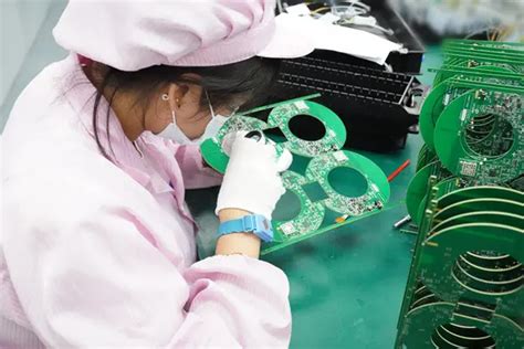
Effective PCB assembly design hinges on balancing precision, manufacturability, and cost-efficiency. By prioritizing Design for Manufacturing (DFM) principles, engineers can minimize production errors while enhancing the reliability of PCBA outcomes. Below are critical insights for optimizing this process:
- DFM Compliance: Aligning designs with manufacturing capabilities reduces rework and accelerates time-to-market. Critical checks include pad spacing, solder mask alignment, and component placement.
- Error Reduction: Automated tools like design rule checks (DRC) and automated optical inspection (AOI) streamline validation, catching issues early in the PCB assembly workflow.
- Material Selection: Choosing substrates and finishes that match operational demands (e.g., high-frequency or high-temperature environments) ensures long-term performance.
"A design that looks perfect on-screen may fail in production without rigorous DFM analysis." – Industry Expert
| Aspect | Traditional Approach | Optimized Approach | Benefit |
|---|---|---|---|
| DFM Compliance | Post-design adjustments | Integrated DFM checks | 30% faster prototyping |
| Material Choice | Standard FR-4 | High-Tg or Rogers substrates | Improved thermal stability |
| Testing | End-of-line inspection | In-process automated testing | 50% fewer defects |
Pro Tip: Collaborate with PCBA manufacturers during the design phase to validate material compatibility and assembly tolerances. This alignment reduces thermal stress risks and ensures seamless scaling from prototype to mass production.
By embedding DFM strategies into every stage, teams achieve cost-efficient production without compromising the precision required for high-performance electronics.
PCB Assembly DFM Compliance Strategies
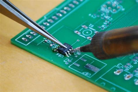
Achieving DFM (Design for Manufacturability) compliance in PCB assembly requires a systematic approach that harmonizes design intent with production realities. At its core, design-phase validation ensures that PCBA layouts align with fabrication and assembly capabilities, minimizing rework and delays. Critical strategies include optimizing component placement to avoid soldering conflicts, adhering to minimum trace width standards for signal integrity, and validating material compatibility with reflow profiles.
A robust DFM checklist should incorporate automated design rule checks (DRCs) to flag issues like insufficient pad spacing or improper via placement. For instance, integrating thermal relief pads in high-current paths prevents solder wicking while maintaining thermal stability. Collaboration with PCB assembly partners during early design stages further refines tolerances and stack-up configurations, ensuring designs meet both performance and manufacturability benchmarks.
Proactive DFM analysis tools can simulate assembly outcomes, identifying risks such as tombstoning or voiding in BGA packages. By prioritizing standardized component libraries and avoiding exotic footprints, designers reduce reliance on custom tooling, lowering costs. Finally, aligning PCB assembly workflows with IPC-7351 and IPC-A-610 standards guarantees consistency in solder joint quality and mechanical durability, laying the foundation for scalable, high-yield production.
Streamlining DFM Processes in PCB Assembly
Effective PCB assembly relies on integrating Design for Manufacturing (DFM) principles early in the development cycle. By aligning design choices with production realities, engineers can minimize costly rework and delays. A streamlined DFM approach begins with optimizing component placement to avoid signal interference and thermal stresses, while ensuring adequate spacing for automated PCBA soldering processes. Leveraging standardized footprints and avoiding overly complex layouts further reduces risks during fabrication.
Collaboration between design and manufacturing teams is critical. Tools like automated DFM checks identify issues such as insufficient annular rings or mismatched pad sizes before prototypes are built. This proactive workflow not only accelerates time-to-market but also enhances yield rates by addressing tolerance mismatches and material compatibility challenges. For instance, selecting PCB assembly materials with compatible thermal expansion coefficients prevents warping during reflow soldering.
Additionally, incorporating modular design elements simplifies scalability for high-volume PCBA production. By balancing performance requirements with manufacturability constraints, engineers achieve cost-efficiency without compromising reliability. Transitioning to a DFM-centric mindset ensures that every design iteration aligns with the capabilities of modern assembly lines, ultimately driving consistency across batches and reducing waste.
Cost-Efficient PCB Assembly Design Techniques
Achieving cost efficiency in PCB assembly requires balancing design innovation with practical manufacturing constraints. A critical starting point is optimizing component placement to minimize pcba production complexities. By standardizing component sizes and footprints, designers can reduce the need for custom tooling, lowering both time and material expenses. Strategic panelization—grouping multiple boards into a single panel—maximizes substrate utilization, directly cutting material waste and per-unit costs.
Another key strategy involves selecting cost-effective yet reliable materials. For instance, opting for FR-4 substrates over high-frequency alternatives in non-critical applications preserves performance while avoiding unnecessary expenditures. Additionally, aligning trace widths and spacing with standard manufacturing tolerances ensures compatibility with automated PCB assembly equipment, reducing rework risks.
Integrating Design for Manufacturability (DFM) principles early in the design phase is paramount. Simulating assembly workflows through software tools identifies potential bottlenecks, such as awkwardly placed vias or insufficient solder mask clearance, before prototyping. This proactive approach minimizes costly revisions and accelerates time-to-market.
Finally, leveraging modular design architectures allows reuse of validated pcba subcircuits across projects, streamlining development efforts and bulk purchasing advantages. When paired with rigorous testing protocols, these techniques ensure cost savings without compromising reliability—a foundational step toward scalable, high-volume production.

Enhancing Reliability Through Precision PCB Design
Achieving reliability in PCB assembly begins with precision-driven design practices that account for both electrical performance and mechanical stability. By optimizing component placement and trace routing, engineers can minimize signal interference and voltage drops, which are critical for high-performance PCBA systems. Implementing design-for-manufacturing (DFM) principles ensures that layouts align with production capabilities, reducing risks of solder joint failures or thermal stress during assembly. For instance, maintaining adequate clearance between components and avoiding acute angles in traces prevents short circuits and improves manufacturability.
Material selection further reinforces reliability, as high-Tg substrates and copper weights tailored to current loads enhance durability under operational stress. Advanced simulation tools enable real-time validation of thermal and mechanical behaviors, allowing designers to preemptively address hotspots or warping risks. Transitioning seamlessly from design to production, these strategies ensure PCBA integrity across temperature cycles and vibrational environments. By prioritizing precision at every design phase, manufacturers can deliver electronics that meet stringent reliability standards while streamlining PCB assembly workflows for scalable success.

Error Reduction in PCB Assembly Workflows
Minimizing errors in PCB assembly workflows requires a systematic approach that integrates design for manufacturability (DFM) principles with advanced process controls. A critical first step involves optimizing PCBA layouts to avoid common pitfalls like component misalignment or solder bridging. By leveraging automated design validation tools, engineers can flag potential issues—such as insufficient pad spacing or conflicting trace routing—before prototyping, reducing costly rework.
Collaboration between design and manufacturing teams further enhances error prevention. For instance, standardizing footprint libraries and assembly guidelines ensures consistency across PCB assembly stages, while real-time feedback loops enable rapid adjustments to component placement or thermal profiles. Advanced inspection systems, including automated optical inspection (AOI) and X-ray testing, add layers of verification to detect subtle defects in high-density PCBA designs.
Proactive error reduction also hinges on material compatibility analysis. Selecting substrates with thermal expansion coefficients aligned to component materials minimizes stress-related failures during reflow soldering. By embedding these strategies into PCB assembly workflows, manufacturers achieve higher first-pass yields, shorter lead times, and improved reliability in complex electronics production.
Material Selection for High-Performance PCB Assembly
Effective PCB assembly relies on strategic material choices that balance electrical performance, durability, and manufacturability. The substrate material forms the foundation, with options like FR-4, polyimide, and PTFE offering distinct advantages for thermal stability, signal integrity, and mechanical strength. For high-frequency applications, low-loss laminates minimize signal attenuation, while high-Tg (glass transition temperature) materials ensure reliability in elevated-temperature environments.
Copper weight and finish further influence PCBA performance. Heavy copper traces enhance current-carrying capacity, critical for power electronics, whereas surface finishes like ENIG (Electroless Nickel Immersion Gold) or HASL (Hot Air Solder Leveling) optimize solderability and corrosion resistance. Dielectric materials must also align with CTE (Coefficient of Thermal Expansion) values of adjacent components to prevent delamination during thermal cycling.
Transitioning from design to production, material compatibility with PCB assembly processes is paramount. For instance, halogen-free substrates meet environmental regulations but require adjustments in soldering profiles. Similarly, selecting solder masks with appropriate viscosity and cure times prevents defects during reflow. By aligning material properties with DFM (Design for Manufacturing) principles, engineers mitigate risks such as warping or pad lifting, ensuring seamless integration into automated PCBA workflows. This holistic approach bridges design intent with manufacturing reality, enabling robust, high-yield electronics production.
Thermal Management in Precision PCB Assembly
Effective thermal management remains a critical factor in ensuring the long-term reliability of PCB assembly processes. As component densities increase in modern PCBA designs, engineers must address heat dissipation challenges through strategic material selection and layout optimization. High-thermal-conductivity substrates like metal-core PCBs and ceramic-filled laminates provide superior heat transfer, while proper spacing between power components prevents localized hotspots.
Advanced simulations using finite element analysis (FEA) tools enable precise modeling of thermal gradients during the design phase, allowing proactive adjustments before manufacturing. Implementing thermal vias beneath high-power devices and incorporating copper pours as heat spreaders further enhances dissipation efficiency. For mission-critical applications, active cooling solutions such as embedded heat pipes or thermoelectric coolers complement passive design strategies.
Manufacturing partners often emphasize design for manufacturing (DFM) guidelines requiring minimum clearance around heat-generating components to facilitate automated assembly. Post-production validation through infrared thermography ensures thermal performance aligns with simulation predictions, reducing field failure risks in high-temperature operating environments.
Testing Protocols for Optimized PCB Manufacturing
Effective PCB assembly workflows rely on rigorous testing protocols to validate design integrity and manufacturing precision. In-circuit testing (ICT) and automated optical inspection (AOI) are critical for identifying solder joint defects, component misalignment, or trace discontinuities in PCBA units. Advanced systems leverage boundary-scan techniques to assess complex circuitry, ensuring compliance with design-for-manufacturability (DFM) guidelines.
Environmental stress screening (ESS) further evaluates PCB assembly resilience under thermal cycling, vibration, and humidity, aligning with industry standards like IPC-A-610. By integrating real-time functional testing, manufacturers verify signal integrity and power distribution, minimizing post-production failures. Statistical process control (SPC) tools analyze test data to refine tolerances and reduce defect rates, directly impacting yield optimization and lifecycle reliability.
Transitioning between design and production phases, these protocols bridge PCBA validation with scalable manufacturing. A structured test coverage plan—prioritizing high-risk components—ensures cost-efficient quality assurance while maintaining alignment with precision-driven design objectives. This systematic approach not only accelerates time-to-market but also strengthens supply chain confidence in high-performance electronics.
Conclusion
In the realm of modern electronics manufacturing, PCB assembly design serves as the cornerstone of product success. A precision-driven approach to PCBA development ensures that design-for-manufacturability (DFM) principles are deeply embedded throughout the engineering lifecycle. By aligning PCB assembly design strategies with rigorous DFM standards, manufacturers achieve optimal balance between functional complexity and production feasibility. This synergy minimizes post-production revisions while enhancing assembly accuracy and long-term reliability. Critical factors such as thermal dissipation optimization, material compatibility, and signal integrity preservation must remain central to design iterations. Furthermore, integrating automated testing protocols early in the PCBA workflow reduces latent defects, ensuring compliance with industry benchmarks. As technological demands escalate, adopting a holistic view of PCB assembly processes—from schematic validation to final inspection—becomes imperative for sustaining competitive advantage in high-performance electronics markets.
FAQs
What are the critical DFM guidelines for successful PCB assembly?
Adhering to design for manufacturability (DFM) principles ensures seamless translation of designs into functional PCBA. Key guidelines include maintaining proper pad-to-hole ratios, avoiding component overcrowding, and aligning with your manufacturer’s capability limits for trace widths and layer counts.
How does material selection impact PCB assembly reliability?
Choosing high-quality substrates, copper weights, and solder masks directly affects thermal performance and signal integrity. For instance, FR-4 remains popular for balanced cost and durability, while specialized materials like polyimide excel in high-temperature environments.
What steps minimize errors in PCBA workflows?
Automated design rule checks (DRCs), comprehensive Bill of Materials (BOM) validation, and prototyping with functional testing reduce discrepancies. Collaboration between design and manufacturing teams early in the process further mitigates risks.
Why is thermal management vital in precision PCB assembly?
Poor heat dissipation can lead to premature component failure. Strategies like thermal vias, copper pours, and strategic placement of heat sinks ensure stable operation, particularly in high-power or densely packed designs.
How do testing protocols enhance PCBA quality?
In-circuit testing (ICT), automated optical inspection (AOI), and environmental stress screening (ESS) identify latent defects. These protocols validate electrical performance and durability, aligning with industry standards like IPC-A-610.
Explore Advanced PCB Assembly Solutions
For tailored support in optimizing your PCB assembly design, please click here to connect with experts specializing in precision-driven manufacturing workflows.