Precision-Driven PCB Assembly Strategies for High-Yield Production
Key Takeaways
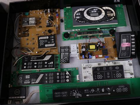
Effective PCB assembly relies on precision-driven strategies that balance manufacturing efficiency with uncompromising quality assurance. Central to achieving high-yield production is the integration of automated inspection systems, which minimize human error while accelerating throughput. For PCBA workflows, selecting high-reliability components and optimizing solder paste application are critical to reducing defects. Advanced methodologies like automated optical inspection (AOI) and X-ray testing ensure thorough validation of solder joints and component alignment, directly impacting long-term product performance.
Equally vital is the alignment of material selection with design specifications, as mismatched thermal or electrical properties can derail even the most meticulously planned assemblies. By embedding real-time process monitoring into production lines, manufacturers gain actionable insights to refine assembly cycles and preempt bottlenecks. Transitioning to these practices not only elevates yield rates but also strengthens compliance with industry standards, positioning PCB assembly as a cornerstone of reliable electronics manufacturing.
Optimizing PCB Assembly Quality Control Processes
Effective quality control in PCB assembly hinges on integrating advanced inspection protocols with data-driven process adjustments. Modern PCBA lines employ automated optical inspection (AOI) and X-ray testing to detect soldering defects, component misalignment, and micro-cracks at sub-millimeter resolutions. Pairing these tools with in-circuit testing (ICT) ensures electrical functionality validation before final product integration.
Tip: Implement statistical process control (SPC) dashboards to monitor defect trends in real time, enabling rapid corrective actions without disrupting production flow.
A critical factor in maintaining yield rates is material selection. For example, using low-voiding solder paste reduces the risk of latent failures in high-reliability applications. Below is a comparison of common inspection methods:
| Method | Defects Detected | Throughput |
|---|---|---|
| AOI | Solder bridges, missing parts | High |
| X-Ray | Voiding, BGA alignment | Moderate |
| ICT | Electrical shorts/opens | Low |
To minimize human error, many manufacturers now adopt machine learning-powered AOI systems that improve defect recognition accuracy by 30–40% over traditional systems. Additionally, establishing clear acceptance quality limits (AQL) for each PCB assembly stage ensures consistency across batches.
Suggestion: Cross-train quality engineers in both PCBA design principles and manufacturing constraints to bridge gaps between prototyping and mass production.
By aligning inspection workflows with lean manufacturing principles, companies can reduce rework cycles by up to 25% while maintaining compliance with industry standards like IPC-A-610. Continuous feedback loops between testing data and process parameters further refine PCB assembly precision, creating a foundation for scalable, high-yield production.

Automated PCB Assembly for High Efficiency
Modern PCB assembly workflows increasingly rely on automation to achieve high-yield production while minimizing human error. By integrating robotic pick-and-place systems with surface-mount technology (SMT), manufacturers can place components at speeds exceeding 50,000 placements per hour, ensuring precision down to ±25 microns. These systems work in tandem with AI-driven vision inspection tools, which validate component alignment and solder paste application in real time, reducing rework rates by up to 30%.
A critical advantage of automated PCBA lies in its scalability. Modular production lines adapt seamlessly to mixed-volume orders, enabling rapid transitions between prototypes and mass production. For instance, closed-loop feedback mechanisms adjust process parameters dynamically, compensating for thermal variations or material inconsistencies. This agility is further enhanced by IoT-enabled equipment, which collects performance data to predict maintenance needs and optimize cycle times.
However, achieving true efficiency requires harmonizing automation with lean principles. Redundant steps, such as manual board handling, are eliminated through conveyor-integrated workflows, while automated optical inspection (AOI) ensures defects are flagged before downstream stages. As a result, manufacturers report 20-40% faster time-to-market and improved resource utilization, reinforcing automation’s role as a cornerstone of modern PCB assembly strategies.
Advanced PCB Assembly Techniques Explained
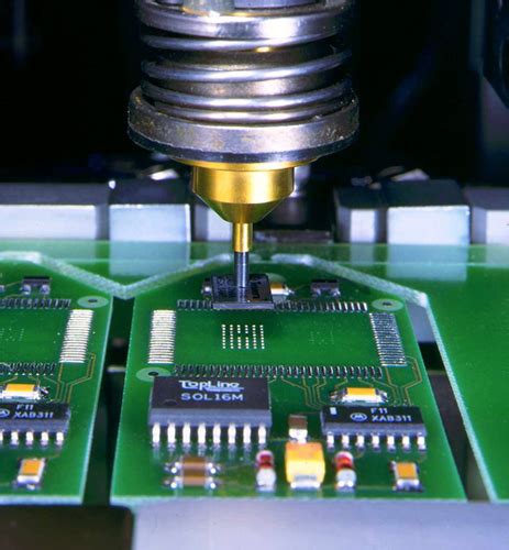
Modern PCB assembly processes leverage cutting-edge methodologies to address the complexities of high-density interconnect (HDI) designs and mixed-technology boards. A cornerstone of advanced PCBA strategies is the integration of automated optical inspection (AOI) systems, which detect microscopic defects like solder bridging or misaligned components with sub-micron precision. Pairing AOI with 3D solder paste inspection (SPI) ensures optimal deposition volume, critical for fine-pitch components such as BGA and QFN packages.
Another breakthrough involves laser direct imaging (LDI), which enhances trace accuracy in high-frequency circuits by eliminating photomasks, reducing registration errors by up to 30%. For thermally sensitive assemblies, vacuum reflow ovens maintain controlled atmospheres, minimizing oxidation while achieving uniform temperature distribution across large panels.
The adoption of sequential lamination techniques allows multilayer boards to meet impedance control requirements in 5G and IoT applications. Additionally, design for manufacturing (DFM) software now incorporates AI-driven simulations to predict and resolve potential assembly conflicts before prototyping.
To ensure scalability, leading manufacturers deploy modular conveyor systems that synchronize pick-and-place machines with curing stations, reducing cycle times by 15–20%. Real-time process monitoring through industrial IoT (IIoT) platforms further optimizes yield rates by correlating production data with quality metrics.
By combining these innovations, PCB assembly workflows achieve unprecedented repeatability, enabling first-pass yield rates exceeding 98% even for complex PCBA projects. This technical evolution underscores the industry’s shift toward data-driven, precision-focused manufacturing paradigms.
Streamlining PCB Assembly Manufacturing Steps
Efficient PCB assembly workflows rely on systematic optimization of manufacturing stages to eliminate redundancies and enhance throughput. By implementing design-for-manufacturability (DFM) principles early in the PCBA process, engineers can preemptively address layout flaws, component placement conflicts, and thermal management challenges. Automated solder paste application and pick-and-place systems minimize human error, while inline optical inspection (AOI) ensures alignment accuracy before reflow soldering.
Another critical aspect involves standardizing material handling protocols to reduce contamination risks and component misplacement. For high-volume production, modular assembly lines with synchronized conveyor systems enable seamless transitions between surface-mount technology (SMT) and through-hole assembly phases. Real-time data analytics further refine cycle times by identifying bottlenecks in solder paste stenciling or component feeding.
To maintain consistency, manufacturers often adopt closed-loop feedback mechanisms between testing stations and assembly equipment. This allows immediate adjustments to parameters like soldering temperature or placement pressure, directly impacting PCB assembly yield rates. Additionally, lean inventory practices—such as just-in-time (JIT) component sourcing—prevent delays caused by material shortages or obsolete parts.
By integrating these strategies, PCBA providers achieve shorter lead times without compromising precision, ensuring scalable solutions for complex electronics manufacturing.
High-Yield PCB Assembly Best Practices
Achieving high yields in PCB assembly hinges on integrating proven methodologies with data-driven process optimization. A foundational step involves rigorous design for manufacturability (DFM) analysis to identify potential bottlenecks early. By aligning component placement, solder mask design, and thermal management with PCBA production capabilities, manufacturers reduce rework rates by up to 35% in high-volume scenarios.
Process validation remains critical—each stage, from solder paste application to reflow profiling, must undergo statistical verification. Implementing automated optical inspection (AOI) systems ensures micron-level accuracy in detecting soldering defects, while predictive maintenance schedules for pick-and-place machinery minimize unexpected downtime. For mixed-technology boards, combining laser-cut stencils with nitrogen-reflow environments improves joint integrity, particularly for fine-pitch components.
Material selection directly impacts yield stability. High-reliability PCB assembly lines prioritize low-voiding solder pastes and moisture-sensitive component baking protocols. Real-time monitoring of process parameters—such as conveyor speed variations within ±0.2%—enables immediate corrections before defects propagate.
Transitioning to high-yield PCBA also demands workforce training on lean manufacturing principles. Cross-functional teams analyzing first-pass yield metrics can pinpoint root causes, whether in stencil aperture design or component tombstoning tendencies. By harmonizing these strategies, manufacturers consistently achieve >98.5% throughput efficiency while maintaining IPC-A-610 Class 3 standards.
Precision Testing in PCB Assembly Lines
Modern PCB assembly workflows rely on precision testing methodologies to ensure consistent quality and reliability in high-volume production. At critical stages of PCBA, automated optical inspection (AOI) systems scan boards at micron-level resolutions, identifying defects like misaligned components, solder bridging, or insufficient paste deposition. Complementing AOI, X-ray inspection provides non-destructive analysis of hidden connections, particularly for ball grid arrays (BGAs) and multilayer boards.
To validate functional performance, in-circuit testing (ICT) and functional circuit testing (FCT) simulate real-world operating conditions, verifying signal integrity and power distribution across complex circuits. Advanced PCB assembly lines integrate machine learning algorithms to refine testing parameters dynamically, reducing false positives while capturing subtle anomalies. For mission-critical applications, environmental stress screening (ESS) subjects assemblies to thermal cycling and vibration tests, exposing latent failures before deployment.
By embedding statistical process control (SPC) tools, manufacturers correlate test data with production variables, enabling rapid root-cause analysis. This closed-loop approach minimizes rework cycles and strengthens yield rates, ensuring that PCBA outputs meet stringent industry standards without compromising throughput.
PCB Assembly Material Selection Impact
The choice of materials in PCB assembly fundamentally shapes product reliability, performance, and manufacturability. From substrate laminates to solder alloys, each component must align with the electrical, thermal, and mechanical demands of the final application. For instance, selecting FR-4 substrates with optimal glass transition temperatures (Tg) ensures dimensional stability during high-temperature PCBA processes, while specialty materials like polyimide cater to flexible or high-frequency designs.
Solder paste composition directly determines joint integrity, with lead-free alloys (e.g., SAC305) balancing environmental compliance and thermal cycling endurance. Similarly, copper weight and surface finishes—such as ENIG (Electroless Nickel Immersion Gold) or HASL—affect signal integrity and corrosion resistance. Component packaging materials, including moisture-sensitive ICs, require precise compatibility with reflow profiles to prevent delamination or tombstoning.
Advanced PCB assembly workflows now integrate material databases and simulation tools to predict interactions between dielectric constants, coefficients of thermal expansion (CTE), and assembly stresses. By aligning material properties with design specifications, manufacturers mitigate risks like warpage or electromigration, directly boosting yield rates. This strategic approach ensures that PCBA outcomes meet both functional benchmarks and cost-efficiency targets, particularly in industries like aerospace or medical electronics where material failures carry critical consequences.
Transitioning to subsequent phases, this material-centric foundation enables tighter integration with automated assembly systems and precision testing protocols, reinforcing end-to-end quality control.
Conclusion
In modern electronics manufacturing, achieving high-yield production hinges on precision-driven strategies that align PCB assembly (PCBA) processes with rigorous quality standards. By integrating automated systems and data-driven methodologies, manufacturers can minimize defects while maximizing throughput across PCB Assy lines. The interplay between advanced material selection, optimized solder techniques, and real-time testing protocols ensures consistent performance in complex circuit configurations.
Ultimately, the success of PCB assembly workflows depends on balancing speed with meticulous attention to detail. Lean manufacturing principles, paired with AI-powered inspection tools, create a framework for identifying inefficiencies before they escalate. This approach not only reduces waste but also strengthens compliance with industry certifications. For businesses aiming to scale, adopting high-yield PCB Assy practices becomes a competitive differentiator, enabling faster time-to-market without compromising reliability.
As technology evolves, continuous refinement of PCBA processes—from component sourcing to final validation—will remain critical. Collaboration between design engineers and production teams ensures that manufacturability is prioritized early, avoiding costly rework. By embedding precision at every stage, manufacturers can sustainably meet the growing demand for high-performance electronic systems.
FAQs
What distinguishes PCB assembly from PCBA?
PCB assembly refers to the process of populating a bare circuit board with components, while PCBA (Printed Circuit Board Assembly) denotes the completed, functional unit ready for integration into electronic devices.
How does automated inspection ensure high-yield production in PCB assembly?
Automated optical inspection (AOI) and X-ray testing identify defects like misaligned components or solder bridging, reducing human error and ensuring manufacturing consistency for high-efficiency PCBA workflows.
Why is material selection critical in precision-driven assembly?
Materials like high-Tg substrates or halogen-free laminates directly impact thermal stability and signal integrity. Proper selection minimizes thermal stress and ensures reliable PCBA performance in demanding environments.
What role do precision testing protocols play in quality control?
Rigorous functional, in-circuit, and environmental testing validates electrical performance under extreme conditions, ensuring compliance with industry standards and reducing field failure rates.
How can manufacturers minimize defects during high-volume PCB assembly?
Implementing statistical process control (SPC) for solder paste deposition, maintaining cleanroom standards, and using nitrogen reflow ovens optimize yield rates by addressing microscopic process variations.
Optimize Your PCB Assembly Workflow Today
Ready to elevate your electronics manufacturing? Click here to explore tailored PCB assembly solutions that align with your production goals.