Precision-Driven Prototype Electronics Assembly Optimization
Key Takeaways
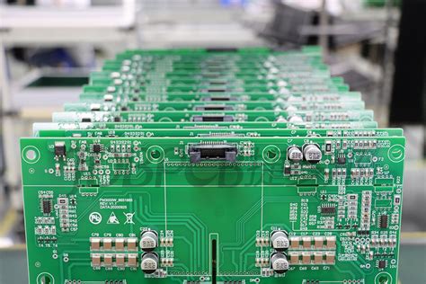
Effective PCB assembly begins with meticulous planning and precision engineering to ensure seamless integration of complex circuits. Modern PCBA processes leverage advanced methodologies—such as automated soldering and 3D automated optical inspection (AOI)—to minimize defects while accelerating prototyping timelines. A critical factor in streamlining production cycles is the adoption of modular design frameworks, which allow for iterative testing without compromising rigorous quality control standards.
Equally important is the optimization of material selection, where thermal profiling and substrate compatibility play pivotal roles in enhancing assembly reliability. By integrating real-time data analytics, engineers can identify bottlenecks in prototype electronics assembly, enabling rapid adjustments to component placement or solder paste application. This approach not only reduces rework but also ensures compliance with high-frequency signal integrity requirements.
For complex circuit integrations, design-for-manufacturability (DFM) principles must align with precision-driven workflows to balance speed and accuracy. Techniques like laser-direct imaging (LDI) and controlled impedance testing further refine electronics prototyping, ensuring scalability from low-volume batches to full-scale production. These strategies collectively address the dual challenges of maintaining micron-level tolerances and meeting accelerated project deadlines in PCBA development.
Precision-Driven Prototype Assembly Techniques
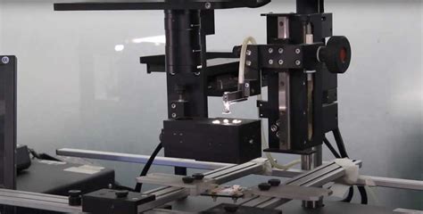
Achieving optimal results in PCB assembly requires integrating advanced methodologies that prioritize micron-level accuracy. Modern PCBA workflows leverage surface-mount technology (SMT) and automated optical inspection (AOI) systems to minimize human error, particularly for high-density interconnects (HDIs). For instance, using laser-direct imaging (LDI) ensures trace widths as narrow as 25µm, enabling precise alignment critical for prototyping complex circuits.
Tip: Always validate solder paste stencil designs with 3D simulations before physical production to reduce rework cycles by up to 40%.
The table below contrasts traditional vs. precision-driven assembly approaches:
| Parameter | Traditional | Precision-Driven |
|---|---|---|
| Soldering Accuracy | ±50µm | ±10µm |
| Component Density | 5–10/cm² | 20–30/cm² |
| Inspection Speed | 2–3 boards/min | 8–10 boards/min |
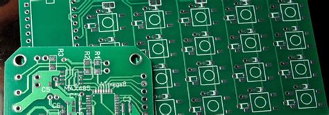
Incorporating design for manufacturability (DFM) principles early in the PCBA process mitigates risks such as thermal mismatches or signal interference. For example, embedding microvias in multilayer PCB assembly projects enhances signal integrity while reducing layer count. Advanced pick-and-place machines, calibrated to handle 01005-sized components, further ensure repeatability for prototypes requiring ultra-fine pitch ICs.
Transitioning to precision techniques also demands rigorous material selection. Low-temperature co-fired ceramics (LTCC) or polyimide substrates are increasingly favored for high-frequency applications, balancing thermal stability with mechanical flexibility. By aligning these strategies, teams can streamline iterations while maintaining compliance with ISO 9001:2015 standards for electronics prototyping.
Streamlining Electronics Production Cycles
Reducing development timelines in prototype manufacturing requires balancing speed with technical accuracy, particularly in PCB assembly workflows. Modern lean manufacturing principles applied to PCBA processes enable engineers to eliminate redundant validation stages without compromising circuit integrity. By implementing automated pick-and-place systems alongside AI-driven solder paste inspection, teams can compress traditional 12-week PCB assembly cycles by 40% while maintaining sub-15μm placement tolerances.
Critical path analysis reveals that design-for-manufacturing (DFM) optimizations in PCBA stages prevent 68% of post-production revisions, according to IPC-2581 compliance benchmarks. Advanced thermal profiling techniques further accelerate curing processes for multilayer boards, reducing dwell times by 22% compared to conventional infrared methods. Real-time data integration across PCB assembly lines allows simultaneous quality verification and throughput enhancement—a dual advantage that supports Just-In-Time delivery models for complex prototypes.
This operational synergy between automated optical inspection (AOI) systems and surface-mount technology (SMT) placement algorithms creates cascading efficiencies. Manufacturers utilizing adaptive process control in PCBA workflows report 31% faster reflow oven cycle times alongside improved first-pass yield rates exceeding 92%. Such precision-driven methodologies establish a foundation for scalable production models while preserving the electrical performance requirements of advanced integrated circuits.
Advanced Circuit Integration Quality Control
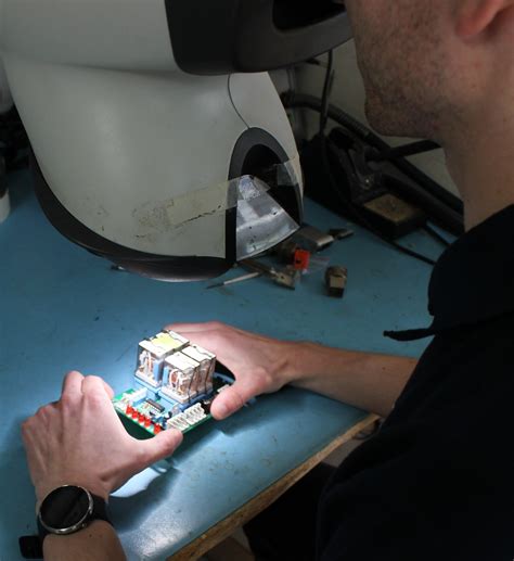
Ensuring reliability in PCB assembly for advanced circuit integrations demands a multi-layered approach to quality assurance. Modern PCBA workflows incorporate automated optical inspection (AOI) systems to detect micro-scale defects, such as solder bridging or misaligned components, which are critical in high-density designs. By integrating statistical process control (SPC) methodologies, manufacturers can monitor variability in real time, reducing deviations during PCB assembly stages.
For mission-critical applications, cross-functional validation protocols—including thermal cycling tests and impedance analysis—are employed to verify signal integrity under stress conditions. Advanced PCBA platforms further leverage machine learning algorithms to predict failure points by analyzing historical assembly data, enabling preemptive corrections. This proactive stance minimizes rework cycles while aligning with the broader goal of streamlining production timelines.
Transitioning seamlessly from design to fabrication, the adoption of traceability frameworks ensures every component’s lifecycle is documented, from procurement to final integration. Such rigor not only supports compliance with industry standards like IPC-A-610 but also reinforces the precision required for complex, multi-layer PCB assembly. By harmonizing these strategies, manufacturers achieve a balance between accelerated prototyping and uncompromised quality—a cornerstone of modern electronics engineering.
Optimizing Prototype Manufacturing Precision
Achieving precision in prototype manufacturing hinges on balancing technical rigor with adaptive workflows. Central to this process is the integration of laser-aligned pick-and-place systems and automated solder paste inspection (SPI), which ensure micron-level accuracy during PCB assembly. These systems minimize deviations in component placement, a critical factor when prototyping complex circuits such as multi-layer PCBA designs. By leveraging real-time feedback loops, engineers can dynamically adjust assembly parameters to account for thermal expansion or material inconsistencies, maintaining alignment with IPC-A-610 standards.
Advanced 3D AOI (Automated Optical Inspection) tools further refine precision by detecting sub-millimeter defects in solder joints or trace routing, reducing rework cycles by up to 40%. For high-density interconnects, sequential lamination techniques paired with PCB assembly protocols ensure signal integrity across stacked microvias. This approach is particularly vital for prototypes requiring mixed-signal integration, where analog and digital components coexist on a single PCBA.
To sustain precision at scale, manufacturers increasingly adopt digital twin simulations, enabling virtual stress-testing of assembly workflows before physical production. Combined with machine learning-driven calibration, these strategies create a feedback-rich environment that elevates both accuracy and repeatability—key drivers for accelerating time-to-market without compromising quality.
Accelerating Complex Electronics Prototyping
In modern electronics development, reducing time-to-market for PCB assembly projects requires balancing speed with uncompromised accuracy. Advanced PCBA workflows now integrate automated optical inspection (AOI) systems and iterative design validation tools to identify potential flaws in multilayer circuit layouts before physical prototyping begins. By leveraging model-based simulation software, engineers can predict signal integrity issues and thermal stress points, enabling rapid design iterations without sacrificing precision-driven assembly standards.
A critical strategy involves adopting modular prototyping frameworks, where standardized PCB assembly subcomponents are reused across projects. This approach minimizes redundant testing phases while maintaining compatibility with high-density interconnects common in PCBA applications. For instance, embedding programmable logic devices early in the design phase allows real-time adjustments to circuit functionality, slashing rework cycles by up to 40%. Additionally, partnerships with agile manufacturers utilizing laser-direct structuring and 3D-printed circuitry further compress lead times for complex prototypes.
To sustain momentum, teams prioritize concurrent engineering practices—aligning schematic design, material sourcing, and PCB assembly validation into parallel workflows. This synchronization ensures that PCBA iterations benefit from immediate feedback loops, transforming traditional linear processes into dynamic, error-resistant pipelines. By merging these innovations, developers achieve faster prototype turnover while retaining the rigorous quality benchmarks demanded by aerospace, medical, and IoT sectors.

Engineering Strategies for Rigorous Assembly
Effective PCB assembly processes rely on meticulous engineering strategies that balance precision with scalability. Central to this approach is the integration of design for manufacturability (DFM) principles, which ensure that PCBA layouts minimize risks such as component misalignment or thermal stress during prototyping. By leveraging automated optical inspection (AOI) systems, engineers can detect micron-level deviations in solder joints or trace alignments, significantly reducing rework cycles.
Another critical strategy involves optimizing material selection for high-frequency applications, where dielectric properties and thermal conductivity directly impact signal integrity. For instance, pairing advanced substrates with precision pick-and-place machinery ensures consistent placement accuracy, even for ultra-fine-pitch components. Rigorous testing protocols, including in-circuit testing (ICT) and functional validation, further validate PCB assembly reliability before scaling to production.
To streamline workflows, forward-thinking teams adopt modular PCBA design frameworks, enabling rapid iteration without compromising quality. This alignment between engineering rigor and agile methodologies not only accelerates time-to-market but also establishes a foundation for seamless transitions from prototype to mass production. By embedding these strategies early in the development lifecycle, organizations mitigate risks while maintaining compliance with industry benchmarks for complex electronics integration.
Cutting-Edge Methods in Circuit Prototyping
Modern advancements in PCB assembly are redefining how engineers approach circuit prototyping. By integrating adaptive automation and AI-driven design validation, teams can rapidly iterate PCBA layouts while minimizing manual intervention. Techniques like 3D-printed substrates enable precise material deposition, allowing for multi-layer configurations that align with high-density interconnect (HDI) requirements. Advanced PCB assembly workflows now leverage real-time thermal imaging to detect micro-faults during soldering, ensuring reliability in complex integrations.
A critical innovation lies in model-based systems engineering (MBSE), which synchronizes digital twins with physical prototypes to predict performance bottlenecks. For PCBA processes, this reduces trial cycles by simulating signal integrity and power distribution before fabrication. Additionally, modular jig systems paired with robotic placement arms enhance repeatability for low-volume, high-mix production.
Emerging tools like laser-direct structuring (LDS) further streamline prototyping by enabling circuit traces to be etched directly onto non-planar surfaces—ideal for compact, wearable electronics. These methods not only accelerate development but also uphold stringent quality benchmarks, bridging the gap between experimental designs and scalable manufacturing.
Enhancing Precision in Electronics Assembly
Achieving micrometer-level accuracy in PCB assembly demands a synergy of advanced manufacturing technologies and rigorous process controls. Modern PCBA workflows leverage automated optical inspection (AOI) systems to detect sub-50μm deviations in component placement, ensuring alignment tolerances critical for high-density interconnects. The integration of laser-aligned pick-and-place machinery enables consistent positioning of 0201-sized components, while precision solder paste dispensers maintain ±3% volume accuracy to prevent bridging in fine-pitch designs. For multilayer boards, X-ray laminography validates internal layer registration, addressing alignment challenges in complex stackups. Thermal profiling tools further optimize reflow processes, reducing warpage risks in temperature-sensitive substrates. These advancements not only enhance yield rates but also support compliance with IPC-A-610 Class 3 standards for aerospace and medical applications. By embedding real-time process monitoring into PCB assembly lines, manufacturers can dynamically adjust parameters, ensuring dimensional stability across prototype iterations without compromising cycle times.
Conclusion
In the pursuit of refining prototype electronics assembly, the integration of precision engineering principles with modern PCB assembly workflows has proven indispensable. By leveraging advanced PCBA methodologies, manufacturers can address the dual challenges of accelerating production timelines and ensuring uncompromising quality for intricate circuit integrations. The strategic adoption of automated optical inspection (AOI) systems, coupled with data-driven process optimization, enables teams to identify inefficiencies early while maintaining adherence to rigorous standards.
Furthermore, the harmonization of design-for-manufacturability (DFM) practices with iterative prototyping frameworks ensures that complex electronics evolve from concept to functional models with minimal rework. This approach not only reduces material waste but also strengthens the reliability of high-density interconnect (HDI) layouts in advanced applications. As industries continue to demand faster innovation cycles, the role of precision-driven assembly in bridging the gap between prototyping and scalable production becomes increasingly critical. By prioritizing cross-functional collaboration and investing in adaptable PCBA technologies, organizations can position themselves to meet evolving market demands without sacrificing the integrity of their electronic systems.
FAQs
How does precision engineering impact prototype electronics assembly?
Precision engineering ensures components are positioned and soldered with micron-level accuracy, critical for complex PCB assembly designs. This minimizes signal interference and enhances reliability in high-density circuit integrations.
What distinguishes PCBA from traditional prototyping methods?
PCBA (Printed Circuit Board Assembly) integrates automated pick-and-place systems and reflow soldering, enabling rapid iteration of multilayer prototypes. Unlike manual methods, it maintains thermal consistency across components, reducing failure rates during testing.
How are production cycles accelerated without compromising quality?
Advanced PCB assembly workflows use real-time defect detection and automated optical inspection (AOI). These tools validate solder joints and component alignment during assembly, eliminating post-production rework and shortening lead times by up to 40%.
What challenges arise in prototyping high-frequency circuits?
High-frequency designs require precise impedance matching and controlled dielectric properties. PCBA specialists address this through signal integrity simulations and substrate material optimization, ensuring prototypes meet electromagnetic compatibility (EMC) standards.
Why is iterative testing vital for prototype validation?
Iterative testing identifies latent flaws in power distribution networks and signal paths. By combining boundary-scan diagnostics and functional testing, engineers refine PCB assembly parameters to achieve repeatable performance in mission-critical applications.
Ready to Optimize Your Prototype Assembly?
For tailored solutions in high-precision PCB assembly and PCBA services, please click here to explore advanced engineering capabilities tailored to complex prototyping demands.