Precision-Driven Strategies for Small Batch PCB Assembly

Key Takeaways
Effective PCB assembly for small batches hinges on balancing cost-efficiency with uncompromised quality. Central to this is adopting precision-driven approaches that streamline prototyping while maintaining rigorous low-volume PCB quality control. A critical consideration is material selection, where prioritizing high-performance substrates and components ensures reliability without inflating expenses.
Tip: Automated PCB assembly solutions (e.g., pick-and-place systems) minimize human error in PCBA, making them ideal for repetitive, low-volume tasks.
For cost-effective testing, combine in-circuit testing (ICT) with functional validation to identify defects early. Below is a comparison of testing methods:
| Testing Method | Cost per Unit | Defect Detection Rate |
|---|---|---|
| Manual Visual Inspection | Low | 60-75% |
| Automated Optical (AOI) | Moderate | 85-95% |
| Functional Testing | High | 95-99% |
When selecting PCB assembly partners, prioritize vendors with expertise in small-batch workflows and certifications like ISO 9001. Reliable partners align with design-for-manufacturability (DFM) principles, reducing rework risks. Finally, integrate iterative prototyping to refine designs before scaling, ensuring alignment between PCB design strategies and production realities.

Small Batch PCB Cost Optimization
Achieving cost efficiency in small batch PCB assembly requires strategic balancing of material choices, process optimization, and supplier partnerships. While prototyping and low-volume production inherently lack economies of scale, adopting design-for-manufacturing (DFM) principles minimizes waste and reduces rework. For instance, optimizing panelization layouts maximizes material usage, directly lowering substrate costs.
Another key strategy involves selecting standardized components over custom parts, which avoids extended lead times and inflated pricing. Partnering with PCBA providers offering tiered pricing models ensures transparency, particularly for batches under 500 units. Crucially, leveraging automated assembly systems—even for small runs—reduces labor-intensive errors, though upfront tooling costs must be evaluated against long-term savings.
Material procurement plays a pivotal role: opting for cost-effective yet reliable substrates (e.g., FR-4 instead of high-frequency laminates) aligns with budget constraints without compromising performance. Additionally, consolidating orders with trusted suppliers often unlocks volume discounts, even for modest batches.
Transitioning to testing, integrating in-circuit testing (ICT) early in the PCB assembly process identifies flaws before full production, preventing costly post-production fixes. This approach dovetails with the broader outline’s focus on quality control and efficient design—ensuring cost optimization doesn’t undermine reliability. By aligning these tactics, manufacturers can navigate the unique challenges of low-volume PCBA while maintaining competitive margins.
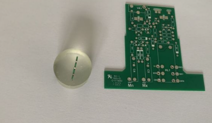
Precision-Driven PCB Prototyping
At the core of effective small batch PCB assembly lies precision-driven prototyping, a process that bridges conceptual designs and functional electronics. Unlike mass production, prototyping demands meticulous attention to design tolerances, material compatibility, and signal integrity to ensure first-iteration success. Advanced PCBA workflows leverage automated optical inspection (AOI) and 3D solder paste monitoring to identify micron-level deviations early, minimizing rework costs.
For specialized applications—such as high-frequency circuits or embedded systems—prototyping requires adaptive design rules that balance performance with manufacturability. Engineers often prioritize controlled impedance routing and thermal management in PCB assembly layouts, using simulation tools to predict real-world behavior. Collaborating with PCBA partners who offer rapid turnaround and design-for-manufacturing (DFM) feedback further refines prototypes, ensuring scalability into low-volume production.
This approach not only accelerates validation cycles but also reduces risks in transitioning from prototype to small batch PCB assembly. By integrating precision at every stage—from schematic verification to post-assembly testing—teams achieve functional reliability without compromising cost-efficiency, a critical advantage in industries like medical devices or aerospace electronics.

Low-Volume PCB Quality Control
Maintaining rigorous quality standards in PCB assembly for low-volume production requires a tailored approach that prioritizes precision without compromising scalability. Unlike high-volume manufacturing, small batch PCBA demands meticulous attention to process controls, as even minor defects can disproportionately impact limited production runs. Critical steps include implementing automated optical inspection (AOI) systems to detect soldering flaws and misalignments, paired with X-ray inspection for verifying hidden connections in multilayer boards.
To ensure consistency, manufacturers often integrate statistical process control (SPC) methodologies, analyzing real-time data to identify deviations in component placement or solder paste application. For low-volume PCBA, functional testing protocols—such as in-circuit testing (ICT) or boundary-scan techniques—should be customized to validate board performance against design specifications, even for prototype-scale batches.
Material traceability is equally vital, with documentation systems tracking components from procurement to final assembly. This becomes particularly crucial when working with specialized or high-value parts, where counterfeit risks or lot inconsistencies could derail tight production timelines. Partnering with PCB assembly providers that adhere to IPC-A-610 or ISO 9001 standards ensures alignment with industry benchmarks, while modular testing frameworks allow adjustments as designs evolve. By balancing advanced inspection tools with adaptable workflows, low-volume PCBA achieves the reliability of mass production, tailored to niche applications.
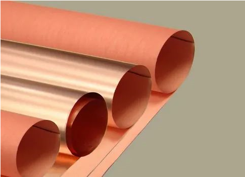
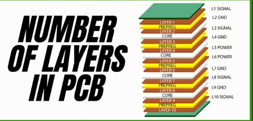
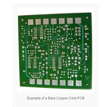
Efficient PCB Material Selection
Selecting optimal materials forms the cornerstone of successful PCB assembly, particularly in small-batch manufacturing where precision and cost constraints intersect. The choice of substrate, copper thickness, and solder mask directly impacts thermal management, signal integrity, and long-term reliability. For high-frequency applications, materials like Rogers or polyimide offer superior performance over standard FR-4, though at a higher cost. Balancing these trade-offs requires evaluating PCBA requirements against production volumes—a critical step for prototyping phases where material over-specification can inflate expenses unnecessarily.
Advanced laminates with low dielectric loss or halogen-free formulations enhance performance in specialized electronics, but their adoption must align with low-volume feasibility. For instance, using high-Tg (glass transition temperature) substrates ensures stability in high-temperature environments, reducing warping risks during reflow soldering. Collaborating with PCB assembly partners early in the design phase helps identify cost-effective alternatives—such as adjusting copper weight or opting for lead-free finishes—without compromising functionality. This strategic alignment between material properties and application demands not only streamlines PCBA workflows but also minimizes waste, a vital consideration for resource-constrained small-batch projects.
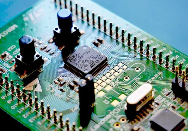
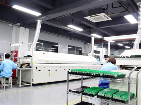
Automated PCB Assembly Solutions
Modern PCB assembly processes increasingly leverage automation to address the unique challenges of low-volume production. Automated PCBA systems integrate robotic pick-and-place machines, precision soldering technologies, and advanced optical inspection (AOI) tools to ensure consistent quality while minimizing human error. For specialized electronics manufacturing, these systems excel in handling complex components like micro-BGA packages or high-density interconnects, which are common in prototyping phases.
A key advantage of automation lies in its ability to streamline workflows without sacrificing flexibility. Programmable machines can rapidly reconfigure for different PCB assembly designs, reducing downtime between batches. This agility is particularly valuable for small-batch orders, where manufacturers must balance tight timelines with exacting technical specifications. Additionally, automated traceability systems track every component’s origin and placement, enhancing compliance with industry standards such as IPC-A-610.
While upfront investments in automation may seem substantial, the long-term gains in yield rates and defect reduction justify the costs. For instance, AOI systems detect soldering flaws or misaligned components at speeds unattainable through manual inspection. When paired with intelligent software, these tools also generate actionable data to refine future PCBA processes. By adopting automated solutions, manufacturers not only meet the demands of precision-driven prototyping but also lay the groundwork for scalable, cost-effective transitions to higher volumes.

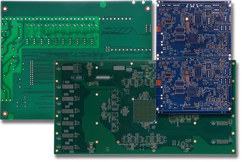
Reliable PCB Design Strategies
Effective PCB assembly begins with foundational design choices that ensure both functionality and manufacturability, particularly in low-volume production scenarios. A robust design strategy prioritizes DFM (Design for Manufacturability) principles, which streamline the transition from prototyping to full-scale PCBA processes. For small-batch projects, this involves optimizing component placement to minimize signal interference, selecting trace widths that balance current capacity with spatial constraints, and incorporating test points for efficient quality validation.
Advanced software tools like automated routing algorithms and thermal simulation platforms enable designers to preemptively address potential failure points, reducing rework costs during PCB assembly. Collaboration with PCBA partners early in the design phase ensures alignment on material compatibility and process capabilities—critical when working with specialized substrates or high-density interconnects. Additionally, modular design frameworks allow for scalable adjustments, accommodating iterative improvements without overhauling entire layouts.
By embedding reliability into the design stage, manufacturers mitigate risks in subsequent phases, from PCB assembly to final testing. This proactive approach not only accelerates time-to-market but also reinforces consistency across small-batch orders, aligning with the precision-driven demands of specialized electronics manufacturing.
Cost-Effective PCB Testing Methods
Implementing cost-effective PCB testing methods is critical for maintaining quality in small batch PCB assembly without compromising budgetary constraints. Automated optical inspection (AOI) systems provide rapid defect detection for PCBA components, reducing manual inspection time by up to 70% while ensuring solder joint integrity. For functional validation, in-circuit testing (ICT) targets specific circuit functionalities, identifying issues like short circuits or open connections early in the prototyping phases. Combining flying probe testing with modular test jigs further optimizes costs for low-volume runs, as these methods require minimal hardware customization.
Strategic use of design-for-test (DFT) principles during layout stages enhances test coverage efficiency, allowing engineers to focus on critical failure points in PCB assembly workflows. Partnering with manufacturers offering scalable testing solutions ensures alignment between prototype validation and mass production requirements. By integrating these approaches, developers achieve reliable performance metrics while avoiding overinvestment in unnecessary test infrastructure—a vital balance for specialized electronics projects with tight margins.
Selecting PCB Assembly Partners
Choosing the right PCB assembly partner is critical for ensuring cost-effectiveness and quality consistency in small-batch production. When evaluating potential PCBA providers, prioritize firms with proven expertise in handling low-volume, high-mix projects. Look for certifications such as ISO 9001 or IPC-A-610 compliance, which validate adherence to industry standards for soldering, component placement, and testing.
A partner’s technical capabilities should align with your project’s complexity—ask about their experience with advanced packaging technologies or mixed-signal designs if required. Supply chain transparency is equally vital; suppliers with robust relationships with component distributors minimize risks of delays or counterfeit parts. For prototyping phases, opt for partners offering design for manufacturability (DFM) feedback to refine layouts before full-scale production.
Additionally, assess their scalability—while focusing on small batches now, ensure they can support volume increases without compromising turnaround times. Flexible PCB assembly services, such as just-in-time inventory management or on-demand build-to-order models, help balance upfront costs with responsiveness. Finally, review their quality assurance protocols: automated optical inspection (AOI) and functional testing should be standard even for low-quantity orders. By aligning these factors, manufacturers secure reliable PCBA collaborations that bridge precision-driven prototyping and scalable production.
Conclusion
In the realm of specialized electronics manufacturing, adopting precision-driven approaches to small batch PCB assembly ensures a critical balance between cost-effectiveness and performance. By integrating advanced PCBA techniques with rigorous quality protocols, manufacturers can address the unique challenges of prototyping and low-volume production. Emphasizing strategic material selection and automated assembly solutions not only streamlines workflows but also reduces waste, aligning with lean manufacturing principles.
The success of PCB assembly in limited quantities hinges on meticulous design validation and real-time testing, which safeguard against defects while maintaining scalability. Partnering with experienced PCBA providers who prioritize transparency and adaptability further strengthens outcomes, particularly when navigating complex technical specifications or tight timelines. Ultimately, the convergence of innovation and practicality in small batch PCB assembly empowers businesses to deliver high-reliability electronics without compromising on efficiency—a necessity in today’s fast-evolving technological landscape.
FAQs
How does small-batch PCB assembly differ from high-volume production?
Small-batch PCB assembly prioritizes flexibility and rapid iteration, allowing adjustments between production runs. Unlike high-volume PCBA, it minimizes upfront tooling costs while maintaining precision for prototyping or niche applications.
What factors influence costs in low-volume PCBA projects?
Key cost drivers include material selection, design complexity, and testing requirements. Optimizing panelization and leveraging automated PCB assembly workflows can reduce expenses without compromising quality.
How is quality ensured in small-batch manufacturing?
Advanced inspection methods like automated optical testing (AOI) and functional verification protocols are critical. Reputable partners combine these with DFM (Design for Manufacturability) reviews to preempt defects.
Can specialized materials be used in low-volume runs?
Yes. Small-batch PCBA allows experimentation with high-frequency or thermal-resistant substrates. However, material availability and lead times should be evaluated early to avoid delays.
What should I look for in a PCB assembly partner?
Prioritize providers with expertise in mixed-technology assembly (SMT/THT) and transparent communication. Certifications like ISO 9001 and IPC-A-610 compliance indicate adherence to quality control standards.
Explore Customized Solutions for Your Project
For tailored PCB assembly strategies that align with your prototyping or low-volume needs, please click here to consult our engineering team.