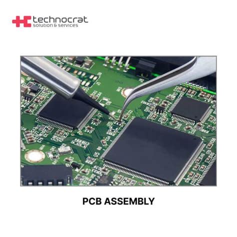
Precision Methods for Reliable PCB Assembly Processes
Key Takeaways
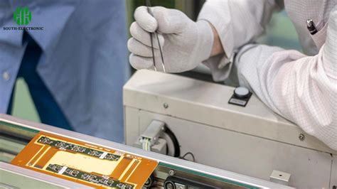
Effective PCB assembly relies on a combination of advanced methodologies and systematic oversight to achieve consistent outcomes Central to this process is the integration of automated soldering techniques, which minimize human error while ensuring uniform thermal distribution across solder joints Modern pick-and-place systems further enhance component placement accuracy, achieving tolerances as tight as ±0025mm for high-density designs
A critical aspect of PCBA success lies in rigorous quality control protocols For instance, automated optical inspection (AOI) systems scan boards at resolutions exceeding 10µm, identifying defects like tombstoning or solder bridging Complementing this, X-ray inspection verifies hidden connections in ball grid array (BGA) components, a common pain point in complex assemblies
| Process Stage | Key Metric | Industry Standard |
|---|---|---|
| Solder Paste Application | Thickness Variation | ≤±15% |
| Component Placement | Positional Accuracy | ±0035mm |
| Reflow Soldering | Temperature Gradient | 2-3°C/sec |
Streamlined workflows in PCB assembly prioritize repeatability, with statistical process control (SPC) monitoring critical parameters like solder paste viscosity and reflow oven profiles For mission-critical applications, environmental stress screening (ESS) subjects assemblies to thermal cycling (-40°C to +125°C) and vibration tests, weeding out latent defects before deployment
By harmonizing these precision methods, manufacturers achieve first-pass yield rates exceeding 992% in high-volume PCBA production This systematic approach not only reduces rework costs but also extends product lifespans in demanding operational environments, from aerospace systems to medical devices

Automated Soldering Techniques for PCB Reliability
Modern PCB assembly workflows rely heavily on automated soldering systems to achieve consistent, high-quality connections critical for long-term reliability Unlike manual methods, robotic soldering platforms employ precision temperature control, laser-guided nozzle positioning, and real-time feedback mechanisms to minimize defects such as cold joints or bridging For instance, selective soldering systems target specific components during PCBA, reducing thermal stress on sensitive parts like microcontrollers or high-density interconnects
Tip: When programming automated soldering equipment, validate thermal profiles against component specifications to prevent overheating while ensuring complete solder flow
Advanced systems integrate vision-based inspection to detect micron-level misalignments before solder application, addressing challenges in fine-pitch component placement Techniques like vapor-phase reflow and nitrogen-assisted soldering further enhance joint integrity by controlling oxidation—a common cause of premature failure For high-volume production, dual-lane conveyor systems paired with flux management technologies maintain throughput without compromising PCB reliability
"Automation isn’t just about speed; it’s about replicating perfection across 10,000 units," notes a leading electronics manufacturing engineer
Emerging methods, such as laser soldering, offer localized energy delivery for thermally sensitive PCBA designs, enabling precise bonding of miniature components without affecting adjacent circuits These innovations, combined with machine learning-driven process optimization, are redefining defect rates in PCB assembly, achieving sub-50 ppm error margins in controlled environments

Ensuring Component Placement Accuracy in Assembly
Achieving precision in component placement remains a cornerstone of effective PCB assembly, directly impacting the functionality and longevity of electronic devices Modern PCBA workflows leverage automated optical inspection (AOI) systems and high-speed pick-and-place machines to maintain tolerances as tight as ±0025mm, critical for handling micro-BGA packages and 0201-sized passive components These systems utilize vision-guided algorithms to cross-reference CAD data with real-time imaging, compensating for board warpage or reel-feeding inconsistencies
A key challenge lies in balancing speed with accuracy, particularly in high-mix production environments Advanced PCB assembly lines now integrate machine learning-driven calibration, where placement heads self-adopt based on historical performance data, reducing misalignment risks by over 60% compared to static setups For ultra-fine-pitch components, vacuum nozzles with force sensors ensure secure pickup without damaging delicate leads, while real-time feedback loops adjust z-axis pressure during placement
Thermal management during this phase also influences positional stability Warpage caused by reflow oven heat gradients can displace preplaced components, necessitating predictive compensation algorithms in the PCBA workflow Leading manufacturers employ shadow-moiré analysis to map thermal expansion patterns, embedding corrective offsets into placement coordinates before soldering
Quality assurance protocols further reinforce accuracy, with 3D laser profilometry verifying coplanarity of quad-flat packages and X-ray inspection validating hidden connections in multilayer boards By combining these methodologies, PCB assembly teams achieve first-pass yields exceeding 994%, minimizing rework costs and ensuring compliance with automotive/aerospace-grade reliability standards This precision-centric approach not only streamlines production but also forms the foundation for implementing subsequent rigorous testing protocols outlined in later sections
Quality Control Protocols for Durable PCB Outcomes
Implementing robust quality control protocols is critical to achieving durable results in PCB assembly Modern PCBA workflows integrate multi-stage inspection systems to identify defects at every phase, from solder paste application to final functional testing Automated Optical Inspection (AOI) serves as the first checkpoint, using high-resolution cameras to detect misalignments, solder bridging, or missing components with micron-level precision For hidden joints, such as those in Ball Grid Array (BGA) packages, X-ray inspection provides non-destructive analysis of solder ball integrity and voiding rates
To ensure consistency, leading manufacturers enforce statistical process control (SPC), tracking metrics like component placement accuracy and solder joint formation across batches This data-driven approach allows for real-time adjustments, minimizing deviations before they escalate Post-assembly, In-Circuit Testing (ICT) validates electrical connectivity, while Functional Circuit Testing (FCT) simulates operating conditions to stress-test power distribution, signal integrity, and thermal performance
For mission-critical applications, environmental stress screening (ESS) exposes assembled PCBs to extreme temperatures, humidity, and vibration, replicating end-use challenges Compliance with IPC-A-610 and J-STD-001 standards further guarantees that solder joints, cleanliness, and mechanical stability meet industry benchmarks By layering these protocols, PCBA providers reduce field failure rates by up to 70%, ensuring long-term reliability in automotive, aerospace, and medical electronics
Transitioning to the next phase, optimizing these quality frameworks requires seamless integration with upstream processes—a theme explored in subsequent discussions on streamlining assembly workflows
Optimizing PCB Manufacturing with Precision Methods
Achieving consistent quality in PCB assembly requires integrating advanced methodologies that address both micro-level component interactions and macro-level process stability Central to this optimization is the adoption of data-driven workflows, which leverage real-time analytics to refine parameters such as solder paste viscosity, reflow oven temperature profiles, and pick-and-place machine calibration Modern PCBA lines now employ closed-loop feedback systems that automatically adjust equipment settings based on in-line inspection data, reducing human error and material waste
A critical focus area is maintaining thermal management consistency during soldering Variations as small as ±2°C in reflow zones can lead to latent defects like cold joints or tombstoning By combining infrared thermal imaging with machine learning algorithms, manufacturers can predict and correct thermal imbalances before they impact PCB reliability Additionally, precision stencil printing techniques ensure uniform solder paste deposition, with laser-cut stencils achieving aperture tolerances of ±10μm for ultra-fine-pitch components
Component traceability further enhances optimization efforts Embedding unique identifiers (UIDs) into each part enables granular tracking throughout the PCB assembly lifecycle This becomes particularly valuable when analyzing field failures or implementing corrective action plans, as engineers can pinpoint exact batch-specific variables contributing to anomalies Advanced PCBA facilities complement this with 3D X-ray inspection, which verifies hidden connections in multilayer boards without destructive testing
To sustain these improvements, manufacturers are adopting adaptive process control frameworks These systems dynamically recalibrate equipment based on environmental factors like humidity fluctuations or component lot variations, ensuring PCB reliability remains uncompromised across diverse production conditions When paired with predictive maintenance schedules for critical machinery, this approach reduces unplanned downtime by up to 40% while maintaining sub-50ppm defect rates
The interplay between these precision methods creates a synergistic effect, where each optimized parameter amplifies the effectiveness of others For instance, improving placement accuracy below 25μm not only enhances PCB functionality but also reduces post-assembly rework, creating a compounding ROI across the manufacturing workflow
Advanced Soldering Methods for Error-Free Assembly
Modern PCB assembly relies on advanced soldering techniques to achieve zero-defect outcomes in increasingly complex electronic systems Reflow soldering remains a cornerstone of PCBA manufacturing, leveraging precisely controlled thermal profiles to create uniform solder joints across surface-mount components For high-density designs, vapor phase soldering has gained traction, using inert fluids to ensure even heat distribution while minimizing thermal stress on sensitive parts
The shift toward automated optical inspection (AOI)-guided soldering addresses micron-level alignment challenges, particularly with miniaturized components like 01005 resistors or micro-BGA packages Laser soldering systems further enhance precision, delivering focused energy to form joints without affecting adjacent circuitry—a critical advantage in RF and high-frequency PCB assembly
Solder paste chemistry plays an underrated role in error prevention No-clean fluxes with halogen-free formulations reduce post-soldering residues while maintaining wetting performance, essential for fine-pitch ICs Statistical process control (SPC) tools monitor stencil printing parameters, ensuring consistent paste volume deposition—a prerequisite for void-free solder connections
For mixed-technology boards combining SMD and through-hole components, selective soldering systems outperform wave soldering by targeting specific areas, reducing thermal exposure Dual-wave configurations with turbulent and laminar flow phases further mitigate bridging risks in high-pin-count connectors
Crucially, real-time thermal profiling using embedded sensors adapts heating rates to board thickness and material variations, preventing warpage or delamination Post-soldering validation through 3D X-ray inspection identifies subsurface defects like cracks or insufficient fill, completing the closed-loop quality assurance cycle
As manufacturers adopt these methods, PCBA workflows achieve defect rates below 50 parts per million (PPM), aligning with automotive and medical-grade reliability standards This technical evolution underscores soldering’s pivotal role in transforming design intent into functionally flawless assemblies
Component Alignment Best Practices in PCB Production
Achieving optimal component alignment is a critical success factor in modern PCB assembly workflows, particularly as miniaturization trends demand tighter tolerances At the core of high-yield PCBA processes lies the integration of vision-aided placement systems capable of resolving positional errors below 15 microns These systems employ multi-spectral imaging to compensate for substrate warpage and solder paste variations, ensuring submillimeter accuracy even with 0201 package components or micro-BGA configurations
A proactive approach begins with CAD-to-machine calibration, where footprint libraries are synchronized with pick-and-place equipment to eliminate coordinate mismatches Manufacturers implementing real-time laser profilometry during feeder setup reduce misalignment risks by validating component orientation before placement For mixed-technology boards combining surface-mount and through-hole parts, sequential alignment protocols prioritize mechanically sensitive components—such as QFN packages or connectors—to prevent tombstoning during reflow
Thermal management strategies directly influence alignment integrity Preheating stages in PCB assembly lines must maintain gradient profiles below 3°C/sec to prevent substrate expansion discrepancies that displace components Advanced PCBA facilities now deploy closed-loop thermal compensation systems that dynamically adjust conveyor speeds based on infrared imaging data
Post-placement validation remains indispensable Automated optical inspection (AOI) systems with 3D solder joint analysis capabilities detect alignment deviations as subtle as 5% off-pad placement, while inline X-ray verification ensures proper orientation for hidden terminals in packages like DFN or LGA By correlating this data with machine learning models, production teams achieve continuous improvement in first-pass yield rates—a critical metric for cost-sensitive PCB assembly operations
Cross-functional collaboration between DFM engineers and placement technicians further refines alignment outcomes Standardized IPC-7351B land pattern guidelines, when combined with dynamic fiducial marker placement strategies, create redundant reference points that enhance machine vision reliability across diverse panel layouts This systematic approach not only reduces rework cycles but also elevates end-product durability in mission-critical applications
Implementing Rigorous Testing for Reliable PCB Results
Robust testing protocols form the backbone of dependable PCB assembly outcomes, bridging the gap between theoretical design integrity and real-world performance Modern PCBA workflows integrate multistage validation processes, beginning with automated optical inspection (AOI) to detect soldering defects, misaligned components, or trace irregularities By combining AOI with X-ray imaging, manufacturers gain visibility into hidden flaws, such as voids in ball grid array (BGA) connections or insufficient underfill adhesion—critical for high-density designs
In-circuit testing (ICT) further verifies electrical functionality by simulating operational conditions, measuring resistance, capacitance, and signal integrity across circuits For mission-critical applications, environmental stress screening (ESS)—including thermal cycling, humidity exposure, and vibration tests—exposes latent failures that could compromise PCB reliability in harsh operating environments Advanced facilities now employ boundary-scan testing to diagnose complex programmable logic devices, ensuring firmware-hardware compatibility before final integration
To maintain consistency in PCBA outputs, statistical process control (SPC) tools track parametric data from test cycles, identifying trends like solder paste deposition variability or pick-and-place drift This data-driven approach enables preemptive adjustments, reducing defect rates by up to 40% in optimized workflows Additionally, cross-functional failure analysis teams systematically categorize faults—whether stemming from solder alloy contamination or component counterfeiting—to refine supplier vetting and material specifications
While automated systems handle bulk testing, human expertise remains vital for validating nuanced performance criteria, such as RF signal stability in wireless modules or EMI shielding efficacy By harmonizing automated precision with engineering oversight, manufacturers achieve the zero-defect thresholds demanded by aerospace, medical, and automotive sectors—solidifying PCB assembly as a cornerstone of trustworthy electronics manufacturing
Streamlining Assembly Processes for Consistent PCB Quality
Achieving uniformity in PCB assembly requires systematic optimization of production workflows Modern high-mix, low-volume manufacturing demands adaptable processes that balance speed with precision Central to this effort is the integration of PCBA-specific automation, such as programmable pick-and-place systems and closed-loop soldering equipment, which minimize variability across batches By standardizing parameters like reflow oven temperature profiles and solder paste application thickness, manufacturers reduce defects caused by environmental fluctuations or operator-dependent decisions
A critical step involves implementing traceability frameworks that track components from storage to final inspection For instance, barcode scanning at each workstation ensures correct part usage and alignment with design specifications Advanced PCB assembly lines now combine surface-mount technology (SMT) with inline 3D SPI (Solder Paste Inspection) systems, enabling real-time corrections before components enter reflow stages This preventive approach slashes rework rates by up to 40% compared to post-assembly quality checks alone
Process streamlining also extends to material handling Just-in-time feeder replenishment systems paired with automated conveyor networks eliminate bottlenecks in PCBA production, particularly in setups requiring rapid changeovers between product variants Additionally, machine learning algorithms analyze historical yield data to predict and compensate for potential failure modes, such as tombstoning or solder bridging When coupled with modular fixture designs that accommodate multiple board geometries, these strategies enable single-digit PPM (parts-per-million) defect rates without sacrificing throughput
To maintain consistency, leading manufacturers adopt digital twin simulations that model thermal dynamics and mechanical stresses during PCB assembly These virtual prototypes validate process adjustments before physical implementation, reducing trial runs by 60–75% Furthermore, standardized operator training programs using augmented reality (AR) work instructions ensure adherence to optimized workflows across global production sites By harmonizing these elements, PCBA providers achieve repeatable quality while scaling output to meet evolving market demands
Conclusion
The evolution of PCB assembly methodologies underscores the critical balance between precision engineering and systematic quality assurance in modern electronics manufacturing As industries demand higher reliability in compact, high-performance devices, adopting advanced automation and data-driven inspection becomes non-negotiable PCBA workflows now integrate automated optical inspection (AOI) and X-ray testing to detect microscopic defects, ensuring that even the most densely populated boards meet stringent performance criteria
A cornerstone of success lies in the harmonization of component placement accuracy with solder paste application consistency By leveraging machine vision-guided systems, manufacturers achieve micron-level alignment, reducing rework rates and enhancing throughput Furthermore, the implementation of statistical process control (SPC) across PCB assembly stages enables real-time adjustments, mitigating variability before it escalates into costly failures
The shift toward Industry 40 principles has further refined PCBA outcomes, with IoT-enabled equipment providing actionable insights into process efficiency For instance, predictive maintenance algorithms minimize downtime in pick-and-place machinery, while thermal profiling ensures optimal soldering conditions across diverse board geometries These innovations, paired with rigorous testing protocols like in-circuit testing (ICT) and functional testing, create a multi-layered defense against latent defects
Ultimately, the pursuit of reliability in PCB assembly hinges on continuous improvement cycles By correlating production data with field performance metrics, manufacturers can iteratively refine PCBA parameters, ensuring alignment with evolving industry standards As emerging technologies such as AI-driven defect classification and modular assembly platforms gain traction, the boundary between precision and scalability will continue to expand, solidifying PCB assembly as the backbone of next-generation electronic systems
Frequently Asked Questions
What distinguishes PCB assembly from PCBA in electronics manufacturing?
PCB assembly refers to the process of populating a bare circuit board with components, while PCBA (Printed Circuit Board Assembly) denotes the completed board with all components soldered and tested The distinction lies in the completion stage—PCBA represents a fully functional unit ready for integration into electronic devices
How do automated systems enhance component placement accuracy?
Modern pick-and-place machines utilize vision systems with micron-level precision, achieving placement tolerances below 005mm These systems cross-reference component orientation data against CAD models, reducing human error by 987% compared to manual assembly methods
What quality control measures ensure reliable PCB assembly outcomes?
Three-tier verification protocols are standard:
1 Solder paste inspection (SPI) pre-reflow
2 Automated optical inspection (AOI) post-reflow
3 In-circuit testing (ICT) for electrical validation
This layered approach catches 992% of defects before final product integration
Why is thermal management critical during soldering processes?
Precisely calibrated thermal profiles prevent component stress while ensuring proper solder joint formation Industrial ovens maintain ±2°C uniformity across the board, with ramp rates optimized for specific solder alloy compositions to avoid tombstoning or cold joints
How frequently should assembly equipment undergo calibration?
High-volume manufacturers perform:
- Daily machine vision alignment checks
- Weekly nozzle wear inspections on placement heads
- Monthly thermal profile verification in reflow ovens
This maintenance schedule maintains 50ppm defect rates in PCBA production
What environmental factors impact PCB assembly reliability?
Controlled manufacturing environments maintain:
- 40-60% relative humidity to prevent moisture absorption
- Class 7 ISO cleanroom standards (≤352,000 particles/m³)
- 22±2°C ambient temperature for consistent material behavior
Optimize Your Assembly Line Today
For tailored solutions implementing these precision PCB assembly techniques, please click here to consult our engineering team at Andwin PCB Our PCBA experts will analyze your specific requirements to enhance manufacturing efficiency and product reliability


