Precision Multilayer PCB Prototyping for Advanced Circuit Designs
Key Takeaways
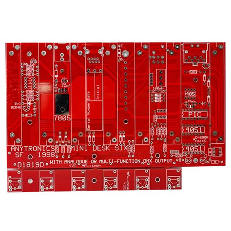
When exploring PCB manufacturing for complex designs, understanding core service elements ensures optimal outcomes. Leading PCB manufacturing companies prioritize rapid prototyping with 3-7 day turnarounds, enabling faster iteration cycles for advanced circuits. For multilayer builds, 8-layer fabrication capabilities paired with FR-4 or rigid-flex materials provide structural versatility, while HDI technology supports high-density interconnects in compact devices.
Tip: Always verify whether your provider offers immersion gold or HASL finishes—the former enhances signal integrity for high-frequency applications, while the latter suits cost-sensitive projects.
Balancing PCB manufacturing cost with quality requires evaluating certifications like ISO compliance, which guarantees adherence to industry standards. For startups in the PCB manufacturing business, partnering with a vendor offering scalable solutions—from prototyping to full production—reduces long-term risks.
Critical considerations include layer alignment precision, material thermal stability, and testing protocols. By aligning these factors with your design requirements, you streamline development timelines and avoid costly revisions. Transitioning smoothly from prototyping to mass production hinges on selecting a partner with expertise in both multilayer engineering and end-to-end PCB manufacturing workflows.
Rapid PCB Prototyping Services
When developing advanced circuit designs, time-to-market often hinges on partnering with PCB manufacturing companies that prioritize speed without compromising quality. Modern rapid PCB prototyping services enable you to test and refine multilayer designs in as few as 3-7 business days, accelerating product development cycles. These services cater to both low-volume validation and pre-production batches, ensuring your PCB manufacturing business stays agile in competitive markets.
Key advantages include:
| Feature | Benefit |
|---|---|
| 3-7 Day Turnaround | Reduces R&D delays |
| 8-Layer Fabrication | Supports complex circuit integration |
| Flexible Material Options | FR-4, Rigid-Flex, or HDI compatibility |
Balancing PCB manufacturing cost with performance requires careful planning. For instance, immersion gold finishes enhance signal integrity in high-frequency applications, while HASL offers a budget-friendly alternative for prototypes. Advanced providers also integrate automated optical inspection (AOI) to ensure ISO-certified standards, minimizing post-production errors.
To optimize your workflow, consider partnering with specialized engineers who tailor solutions to your design’s layer count, material, and finish requirements. This approach ensures your prototypes align with both technical specifications and project timelines, positioning your innovations for scalable success.
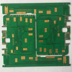
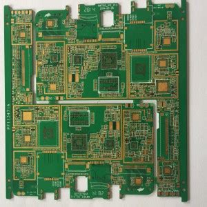
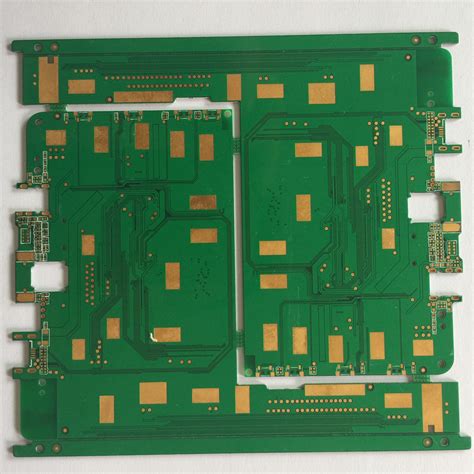
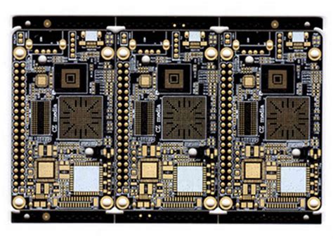
8-Layer Circuit Board Fabrication
When designing advanced electronic systems, 8-layer circuit board fabrication provides the structural complexity required for high-density interconnects and signal integrity. Modern PCB manufacturing processes enable precise stacking of alternating conductive and insulating layers, with specialized via technologies (blind, buried, or microvias) ensuring reliable connections between layers. This complexity demands expertise from PCB manufacturing companies to balance thermal management, impedance control, and material selection—particularly when using high-performance substrates like FR-4 or polyimide.
The PCB manufacturing cost for 8-layer boards depends on factors like copper weight, surface finish (e.g., immersion gold for high-frequency applications), and tolerance requirements. Rigorous testing protocols, including automated optical inspection (AOI) and electrical network testing, mitigate risks in high-layer-count designs. For businesses optimizing their PCB manufacturing business strategy, 8-layer prototypes offer a scalable pathway to volume production while maintaining design flexibility. Advanced fabrication techniques, such as laser drilling and sequential lamination, ensure these multilayered boards meet stringent performance benchmarks without compromising turnaround timelines.
FR-4 and Rigid-Flex PCB Options
When selecting materials for PCB manufacturing, understanding the trade-offs between FR-4 and rigid-flex options ensures your design aligns with performance and budget requirements. FR-4, the industry-standard laminate, offers excellent thermal resistance and mechanical stability for most multilayer prototypes, making it a cost-effective choice for high-volume PCB manufacturing business operations. Its versatility supports designs ranging from simple 2-layer boards to complex 8-layer circuit boards, ideal for applications like consumer electronics or industrial controls.
For advanced projects demanding dynamic form factors, rigid-flex PCBs merge rigid and flexible substrates into a single unit. This eliminates connectors between sections, reducing failure points in space-constrained or high-vibration environments—critical for aerospace or wearable tech. While PCB manufacturing cost increases slightly due to specialized materials and processes, the long-term reliability benefits often justify the investment.
Leading PCB manufacturing companies optimize material selection based on your design’s mechanical stress thresholds and signal integrity needs. For instance, FR-4 suits designs prioritizing thermal management and affordability, while rigid-flex excels in compact, three-dimensional layouts. Always verify that your supplier offers both options with certifications like ISO 9001, as this ensures consistent quality across material types and layer counts.
Immersion Gold vs HASL Finishes
When choosing surface finishes for your multilayer PCB prototype, understanding the trade-offs between Immersion Gold (ENIG) and HASL (Hot Air Solder Leveling) ensures optimal performance and cost efficiency. Immersion Gold provides a flat, uniform surface ideal for fine-pitch components and high-frequency applications, making it a top choice for advanced pcb manufacturing requiring precise signal integrity. Its corrosion-resistant properties also enhance durability in harsh environments. However, pcb manufacturing cost considerations often lead pcb manufacturing companies to recommend HASL, a more economical finish with excellent solderability. While HASL’s uneven surface can pose challenges for ultra-dense designs, its affordability suits high-volume pcb manufacturing business models.
Your decision hinges on balancing technical requirements with budget constraints. For prototypes demanding tight tolerances or extended shelf life, Immersion Gold justifies its higher price. Conversely, HASL remains a practical option for cost-sensitive projects without compromising basic functionality. Always verify compatibility with your assembly process—ENIG’s smooth finish simplifies soldering, while HASL may require additional flux for optimal results. By aligning your finish selection with design goals, you ensure seamless integration into broader pcb manufacturing workflows.
ISO-Certified Quality Assurance
When evaluating PCB manufacturing companies for advanced prototyping, verifying ISO certification ensures adherence to globally recognized quality benchmarks. ISO 9001 and 14001 certifications confirm that a PCB manufacturing business employs rigorous process controls, from material sourcing to final inspection, minimizing defects and ensuring consistency. These standards directly impact PCB manufacturing cost by reducing waste and rework, while maintaining compliance with industry regulations.
For multilayer designs, certified providers implement traceable documentation and automated testing protocols, critical for detecting issues in high-density interconnects or rigid-flex configurations. This level of oversight not only safeguards against electrical failures but also streamlines communication between engineering teams and manufacturers.
It’s worth noting that ISO-certified PCB manufacturing prioritizes supply chain transparency, ensuring materials like FR-4 substrates or immersion gold finishes meet exact specifications. For time-sensitive projects, this systematic approach supports faster turnaround without compromising reliability—a key advantage when scaling prototypes to production. By aligning with certified partners, you mitigate risks associated with design iterations and ensure your multilayer boards perform as intended in demanding applications.
HDI Multilayer Prototyping Solutions
When developing high-density interconnect (HDI) designs, PCB manufacturing processes must adapt to accommodate intricate routing and miniaturized components. HDI multilayer prototyping leverages advanced technologies like laser-drilled microvias and stacked copper layers to achieve finer trace widths (≤75μm) and higher interconnection density—critical for compact devices like wearables or IoT systems. Leading PCB manufacturing companies employ sequential lamination cycles and precision registration systems (±25μm) to ensure signal integrity across 8+ layers, even with rigid-flex configurations.
While PCB manufacturing cost increases with HDI complexity due to additional process steps, the long-term benefits for your product’s performance often justify the investment. For instance, blind/buried vias reduce layer transitions by 40–60%, enhancing signal speed while minimizing electromagnetic interference. When evaluating PCB manufacturing business partners, prioritize facilities offering DFM validation and impedance control testing—these mitigate risks in high-frequency or high-speed applications. By integrating HDI solutions early in prototyping, you avoid costly redesigns while accelerating time-to-market for cutting-edge electronics.
3-7 Day Turnaround PCB Manufacturing
When time-sensitive projects demand rapid execution, partnering with PCB manufacturing companies that offer 3-7 day turnaround becomes critical. This accelerated timeline ensures your advanced circuit designs move from concept to functional prototype without compromising precision or reliability. Modern PCB manufacturing workflows leverage automated processes and advanced machinery to reduce lead times while maintaining strict quality benchmarks—a balance that directly impacts PCB manufacturing cost efficiency.
For businesses prioritizing speed, just-in-time production models enable seamless integration with R&D cycles. However, faster turnarounds require meticulous planning. Factors like layer count, material selection (e.g., FR-4 vs. rigid-flex), and surface finishes (immersion gold or HASL) influence both timelines and PCB manufacturing business outcomes. Leading providers optimize these variables by combining standardized fabrication protocols with flexible scheduling, ensuring even complex 8-layer boards meet tight deadlines.
To maximize value, verify that your manufacturer’s rapid prototyping capabilities align with ISO-certified quality controls. This dual focus on speed and compliance ensures your prototypes are not only delivered quickly but also meet performance expectations for high-density interconnect (HDI) or mixed-signal applications. By aligning with a partner that prioritizes agile PCB manufacturing, you mitigate project risks while accelerating time-to-market for cutting-edge electronics.
Precision Multilayer PCB Engineering
Achieving optimal performance in advanced circuit designs hinges on ## Precision Multilayer PCB Engineering, where every layer alignment, via placement, and material choice directly impacts functionality. When selecting PCB manufacturing companies, prioritize those with expertise in high-density interconnect (HDI) technologies and laser-drilled microvias—critical for minimizing signal loss in complex layouts. Modern PCB manufacturing workflows integrate automated optical inspection (AOI) systems to ensure sub-0.1mm alignment tolerances, essential for 8-layer+ designs requiring rigid-flex compatibility or FR-4 substrate optimization.
The PCB manufacturing cost often correlates with material selection and layer count, but advanced providers leverage panelization techniques to reduce waste. For instance, immersion gold (ENIG) finishes enhance solderability for fine-pitch components, while HASL remains a budget-friendly alternative for prototyping. In the PCB manufacturing business, balancing speed and precision is key: look for suppliers offering 3-7-day turnaround without compromising impedance control or thermal management. By partnering with ISO-certified engineers, you ensure designs meet IPC-6012 Class 3 standards—a non-negotiable for aerospace, medical, or high-frequency applications.
Conclusion
When navigating the complexities of PCB manufacturing for advanced designs, selecting the right partner among PCB manufacturing companies can significantly impact project success. Your choice must balance technical expertise with PCB manufacturing cost considerations, ensuring alignment with both performance requirements and budget constraints. This becomes particularly evident in multilayer prototyping, where factors like layer count, material selection, and surface finishes directly influence functionality and reliability.
Leading PCB manufacturing business providers distinguish themselves through capabilities like 8-layer fabrication and HDI solutions, coupled with certifications that validate quality standards. By prioritizing partners offering rapid turnaround and flexible material options, you accelerate development cycles while maintaining precision. Ultimately, the value lies not just in prototype delivery but in securing a collaborator capable of scaling with your evolving needs—whether optimizing PCB manufacturing cost structures or advancing toward high-volume production.
Frequently Asked Questions
How does multilayer PCB prototyping differ from standard PCB manufacturing?
PCB manufacturing for multilayer prototypes involves stacking multiple conductive layers separated by insulating material, requiring advanced alignment and lamination techniques. Standard processes typically handle simpler designs, while prototyping demands precision for complex circuits like 8-layer fabrication or HDI layouts.
What factors influence PCB manufacturing cost for multilayer prototypes?
Cost depends on layer count, material choice (FR-4 vs. rigid-flex), surface finish (immersion gold or HASL), and turnaround time. High-density interconnects (HDI) or specialized certifications (e.g., ISO) may increase expenses, but many PCB manufacturing companies offer scalable pricing for prototyping.
Why choose specialized PCB manufacturing business partners for prototypes?
Expert providers ensure tighter tolerances, signal integrity, and reliability for advanced designs. They streamline processes like 3-7 day turnaround and offer design feedback, reducing risks before full-scale production.
Can PCB manufacturing handle both rigid and flexible multilayer designs?
Yes, leading suppliers support rigid-flex configurations, combining rigid sections for component mounting with flexible areas for space-constrained applications. This versatility is critical for aerospace, medical devices, or IoT systems.
How do surface finishes impact prototype performance?
Immersion gold offers superior corrosion resistance and solderability for high-frequency circuits, while HASL provides a cost-effective option for less complex boards. Your choice depends on application requirements and PCB manufacturing cost considerations.
Ready to Start Your Project?
For tailored solutions in PCB manufacturing or to discuss your multilayer prototype needs, please click here to connect with our engineering team.


