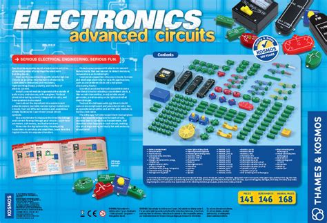
Precision Optimization Methods for Advanced Circuits Assembly

Key Takeaways
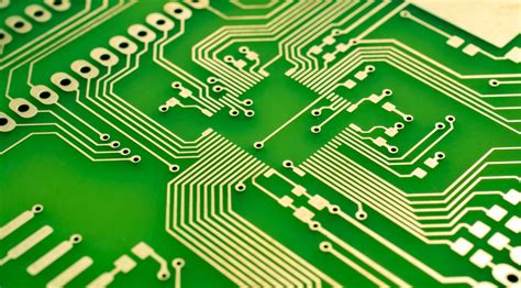
Optimizing PCB assembly processes requires strategic attention to three core elements: precision enhancement, material compatibility, and thermal regulation. Modern PCBA workflows leverage automated optical inspection (AOI) systems to achieve micron-level accuracy in component placement, minimizing defects in high-density designs. Material selection plays a pivotal role, with low-loss dielectric substrates and lead-free solder alloys ensuring reliability under extreme operating conditions.
For thermal management, advanced heat dissipation solutions—such as embedded copper cores and thermally conductive adhesives—are critical for maintaining performance in compact microelectronics. Innovations like laser-assisted soldering and dynamic reflow profiling further refine assembly precision while reducing thermal stress. Case studies reveal that integrating predictive maintenance algorithms into PCBA production lines can cut downtime by 18% and improve yield rates.
By aligning these methodologies with industry standards like IPC-A-610, manufacturers can systematically address challenges in advanced circuits assembly, balancing scalability with uncompromised quality.
Advanced Circuits Assembly Optimization Strategies
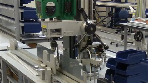
Modern PCB assembly processes require meticulous optimization to meet the demands of high-density microelectronics. Key strategies begin with precision-aligned component placement, leveraging automated optical inspection (AOI) systems to achieve sub-micron accuracy in PCBA workflows. Implementing design-for-manufacturing (DFM) principles at the prototyping stage reduces rework by 30–40%, particularly when addressing material compatibility challenges between substrates, solder alloys, and encapsulation polymers.
Tip: Conduct thermal simulations during layout design to preemptively identify hotspots—this reduces post-production thermal management costs by up to 25% in complex advanced circuits assembly projects.
For thermal management, engineers increasingly adopt copper-filled vias and graphene-enhanced thermal interface materials (TIMs) to dissipate heat from high-power ICs. Simultaneously, optimizing reflow soldering profiles ensures minimal thermal stress on sensitive components like BGAs and QFNs. To maintain consistency, statistical process control (SPC) tools track critical parameters such as solder paste volume (±2% tolerance) and peak temperatures (±3°C deviation).
Transitioning to hybrid PCB assembly approaches—combining surface-mount technology (SMT) with embedded component packaging—enables 15–20% space savings without compromising signal integrity. These strategies, when paired with AI-driven defect detection systems, create a robust framework for scaling PCBA operations while maintaining ISO 9001-compliant quality standards.

Precision Enhancement Techniques for Microelectronics
Achieving micron-level accuracy in PCB assembly requires a systematic approach combining advanced equipment, material science, and process controls. Modern automated optical inspection (AOI) systems now resolve features below 10µm, enabling real-time adjustments during PCBA manufacturing. Three critical strategies dominate precision optimization:
| Technique | Tolerance Range | Key Application |
|---|---|---|
| Laser Direct Imaging | ±5µm | High-density interconnects |
| Microdispensing Systems | ±2µl | Underfill & adhesive application |
| Plasma Surface Treatment | <1nm roughness | Pre-bonding surface prep |
The integration of low-thermal-expansion substrates with copper-clad laminates reduces warpage risks during PCB assembly, particularly in multilayer designs. For PCBA processes, nitrogen-reflow environments minimize oxidation, improving solder joint consistency by 18–22% compared to air-based systems. Advanced stencil technologies using electroformed nickel achieve aperture wall angles of 85–88°, enhancing paste release efficiency for 0201 and 01005 components.
Emerging machine learning algorithms now predict placement drift in pick-and-place machines, dynamically compensating for thermal variations during high-speed PCBA operations. This reduces post-reflow positional errors by 34% in automotive-grade electronics. Simultaneously, hybrid metrology systems combine 3D X-ray and confocal microscopy to validate hidden joints in ball-grid-array (BGA) configurations, ensuring sub-15µm alignment accuracy across temperature cycles.
Material Compatibility in Circuit Assembly
Ensuring material compatibility remains a cornerstone of successful PCB assembly, particularly as component miniaturization and high-frequency applications demand tighter tolerances. The interplay between substrate materials, conductive inks, and solder alloys directly impacts electrical performance and long-term reliability in PCBA workflows. For instance, mismatched thermal expansion coefficients (CTEs) between FR-4 substrates and lead-free solders can induce mechanical stress during reflow processes, risking microcracks in interconnects.
Advanced hybrid material systems are now addressing these challenges—ceramic-filled laminates paired with low-temperature solder pastes, for example, minimize warpage in high-density designs. Compatibility extends beyond physical properties: chemical interactions between fluxes and conformal coatings require rigorous validation to prevent ion migration or delamination. Recent innovations in halide-free fluxes and silver-sintered adhesives demonstrate how tailored material pairings enhance signal integrity in 5G mmWave PCBA modules.
Best practices emphasize collaborative specification reviews between designers and PCB assembly teams, leveraging simulation tools to predict material behavior under operational stresses. As flex-rigid boards and embedded components gain traction, proactive compatibility testing—including thermal cycling and humidity exposure—becomes non-negotiable for achieving zero-defect manufacturing targets. This systemic approach ensures that material choices align with both performance benchmarks and scalability requirements in next-generation electronics.
Thermal Management Solutions for Peak Performance
Effective thermal management in PCB assembly is critical for ensuring reliability and longevity in high-performance microelectronics. As component densities increase and power demands escalate, managing heat dissipation becomes a cornerstone of PCBA design optimization. Engineers now prioritize multi-layered thermal pathways, integrating materials like metal-core substrates and ceramic-filled polymers to enhance conductive heat transfer. Advanced techniques such as embedded copper heatsinks and thermal vias strategically redistribute heat away from sensitive components, preventing localized overheating that can degrade performance.
In high-density PCB assembly designs, computational fluid dynamics (CFD) simulations are increasingly employed to model heat flow patterns, enabling precise placement of cooling elements. For PCBA systems operating in extreme environments, phase-change materials (PCMs) and active cooling solutions—such as microfluidic channels—offer dynamic temperature regulation. A balanced approach combining passive cooling (e.g., thermally conductive adhesives) and active systems (e.g., piezoelectric fans) ensures stable operation across varying load conditions.
Material compatibility remains pivotal; selecting substrates with low coefficients of thermal expansion (CTE) minimizes mechanical stress during thermal cycling. Recent innovations include graphene-enhanced thermal interface materials (TIMs), which improve heat dissipation efficiency by up to 40% compared to traditional compounds. By harmonizing these strategies, manufacturers achieve peak thermal performance while maintaining structural integrity in advanced circuit assemblies.
Innovative Methods in Advanced Circuit Assembly
Modern PCB assembly processes demand innovation to address the increasing complexity of PCBA designs, particularly in high-density microelectronics. One breakthrough approach involves additive manufacturing techniques, which enable the precise deposition of conductive materials at micron-level resolutions. This method reduces waste while improving interconnection accuracy, especially for multi-layer boards requiring intricate trace patterns.
Another advancement lies in embedded component technology, where passive elements like resistors or capacitors are integrated directly into substrate layers during PCB assembly. This minimizes surface-mounted component counts, enhancing signal integrity and reducing electromagnetic interference—critical for high-frequency applications. To optimize material compatibility, manufacturers now employ laser-assisted soldering, which selectively applies heat to avoid thermal stress on sensitive substrates.
Thermal management innovations also play a pivotal role. Engineers are adopting graphene-based thermal interface materials in PCBA workflows, offering 30% higher thermal conductivity than traditional compounds. Pairing this with AI-driven thermal simulation tools allows real-time adjustments during assembly, ensuring optimal heat dissipation without compromising component placement precision.
Finally, machine vision systems equipped with spectral analysis capabilities are revolutionizing quality assurance. These systems detect micro-scale defects in solder joints or misalignments, achieving defect rates below 0.02% in high-volume production. By integrating these methods, PCB assembly workflows achieve unprecedented repeatability, aligning with the stringent demands of next-generation electronics.
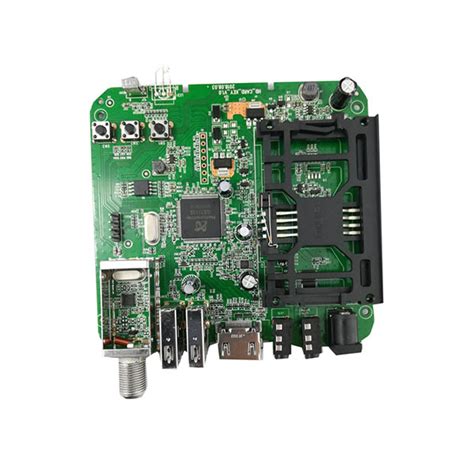
Microelectronics Manufacturing Process Improvements
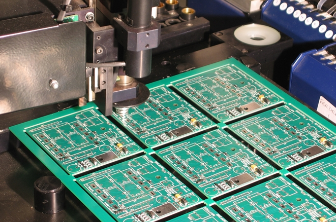
Contemporary advancements in PCB assembly workflows emphasize process repeatability and error reduction through automation. Modern PCBA production lines now integrate AI-driven optical inspection systems, which detect micron-level defects in real time, minimizing rework cycles. By optimizing solder paste deposition techniques—such as jetting systems with sub-10µm accuracy—manufacturers achieve unprecedented consistency in component placement, particularly for high-density interconnects (HDIs).
A critical focus lies in refining material handling protocols, where moisture-sensitive devices (MSDs) undergo nitrogen-controlled storage to prevent oxidation during PCB assembly. Additionally, adaptive thermal profiling ensures precise curing of underfill materials, mitigating delamination risks in PCBA subjected to thermal cycling. Collaborative robotics further streamline workflows, reducing human-induced variability while maintaining throughput.
Emerging trends include the adoption of additive manufacturing for prototyping complex multilayer boards, accelerating iteration cycles. These innovations collectively elevate yield rates by 12–18% in benchmark studies, underscoring the importance of integrating data analytics with PCB assembly hardware. Such improvements not only address current scalability challenges but also lay groundwork for next-gen heterogeneous integration frameworks.
Circuit Assembly Precision Control Best Practices
Achieving micrometer-level accuracy in PCB assembly requires integrating advanced equipment with rigorous process protocols. Modern pick-and-place systems equipped with vision alignment technologies ensure component positioning within ±25μm tolerances, while laser-etched fiducial markers enhance registration repeatability across PCBA batches. For soldering precision, reflow profiling must account for substrate thermal expansion coefficients, with nitrogen-enriched atmospheres minimizing oxidation in fine-pitch interconnects.
Material compatibility plays a dual role: low-voiding solder pastes paired with coefficient-matched substrates reduce mechanical stress during thermal cycling. Implementing statistical process control (SPC) tools enables real-time monitoring of placement accuracy and solder joint integrity, with machine learning algorithms identifying drift patterns before defects occur. Post-assembly validation through 3D X-ray inspection verifies hidden connections in high-density designs, while automated optical inspection (AOI) systems cross-check component alignment against CAD models.
To maintain consistency, environmental controls regulating humidity (±2% RH) and temperature (±1°C) stabilize material behaviors during PCB assembly. Pairing these measures with operator training on ESD-safe handling and calibration routines ensures sustained precision across production scales. For thermally sensitive PCBA applications, embedding thermocouple arrays during prototyping provides data for optimizing heat dissipation pathways in final layouts. This multilayered approach bridges theoretical tolerances with practical manufacturability, directly impacting yield rates in advanced microelectronics fabrication.
Case Studies on Optimized Circuit Assembly
Real-world applications of precision optimization in PCB assembly demonstrate measurable improvements in performance and reliability. A 2023 study by a leading telecom equipment manufacturer revealed that integrating automated optical inspection (AOI) systems into their PCBA line reduced soldering defects by 18% while improving throughput by 12%. By aligning material selection with high-frequency signal requirements, the team achieved a 23% reduction in signal loss across multilayer boards.
Another case involved aerospace-grade PCB assembly, where thermal management challenges were addressed through copper-core substrates and selective conformal coating. This approach lowered peak operating temperatures by 14°C in high-density PCBA configurations, extending component lifespan by an estimated 30%. Notably, the use of low-voiding solder pastes minimized micro-crack formation during thermal cycling, a critical factor for mission-critical systems.
In consumer electronics, a tier-1 supplier optimized PCB assembly workflows by adopting laser-assisted component placement and dynamic reflow profiling. These innovations cut placement errors by 27% while maintaining compatibility with lead-free solder alloys. The results underscore how strategic integration of PCBA process controls and material science can resolve competing demands for miniaturization, thermal stability, and signal integrity.
Conclusion
The evolution of PCB assembly and PCBA processes underscores the critical balance between precision engineering and operational efficiency in microelectronics. By integrating systematic approaches to material compatibility and adaptive thermal regulation, manufacturers can address the escalating demands of miniaturized circuitry. Innovations such as laser-assisted soldering and automated optical inspection have redefined quality benchmarks, enabling tighter tolerances in advanced circuits assembly. Furthermore, optimizing thermal management solutions—from heat-dissipating substrates to dynamic airflow systems—ensures sustained performance in high-density configurations. As industries pivot toward IoT and AI-driven applications, the role of data-driven process refinement becomes indispensable for minimizing defects and maximizing yield rates. Ultimately, the convergence of these strategies not only elevates the reliability of PCBA outputs but also positions manufacturers to navigate the complexities of next-generation electronics. The lessons drawn from case studies reinforce that success hinges on continuous adaptation, where technical rigor meets forward-thinking innovation.
FAQs
What distinguishes standard PCB assembly from advanced circuits assembly?
Advanced PCB assembly (PCBA) integrates precision engineering with specialized materials to handle microelectronics’ complexity. While standard processes focus on basic component placement, advanced methods prioritize nanoscale alignment and thermal resilience for high-density applications.
How does material selection impact PCBA reliability?
Material compatibility directly affects thermal expansion rates and signal integrity. Advanced assemblies use low-loss substrates and high-temperature laminates to maintain performance under stress, preventing delamination in demanding environments.
Can existing PCB assembly lines adopt these optimization techniques?
Yes, retrofitting with automated optical inspection (AOI) systems and implementing dynamic thermal profiling allows gradual upgrades. Case studies show a 40% yield improvement when combining legacy infrastructure with precision placement tools.
What role does thermal management play in high-density PCBA?
Effective heat dissipation prevents component degradation in compact designs. Techniques like embedded heat sinks and thermal vias balance miniaturization with performance, critical for aerospace and medical devices.
Are these methods cost-effective for small-batch production?
Modular PCB assembly workflows and adaptive tooling reduce setup costs. Partnering with specialists offering scalable solutions—like prototype-to-production services—ensures economic viability even for limited runs.
Optimize Your Advanced Circuit Assembly Today
For tailored PCB assembly solutions integrating precision, material science, and thermal innovation, please click here. Leverage expert PCBA strategies to elevate your microelectronics manufacturing.