Precision Requirements in PCB Manufacturing Processes
Introduction
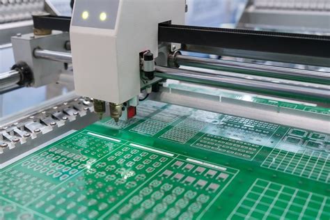
Printed Circuit Board (PCB) manufacturing is a complex process that involves multiple stages, each requiring strict precision to ensure the final product’s functionality and reliability. As electronic devices become smaller and more sophisticated, the demand for high-precision PCBs has increased significantly. This article explores the key precision requirements in PCB manufacturing processes, including material selection, imaging, etching, drilling, plating, and surface finishing.
1. Material Selection and Preparation
The foundation of a high-quality PCB lies in the selection of appropriate base materials, typically copper-clad laminates (CCL). The precision requirements at this stage include:
- Dimensional Stability: The substrate must maintain its shape and size under thermal and mechanical stress. Warping or shrinkage can lead to misalignment in later stages.
- Copper Foil Thickness Tolerance: The copper layer thickness must be uniform, typically ranging from ½ oz (17.5 µm) to 6 oz (210 µm), with tight tolerances (±5%).
- Dielectric Constant Consistency: Variations in dielectric properties can affect signal integrity in high-frequency applications.
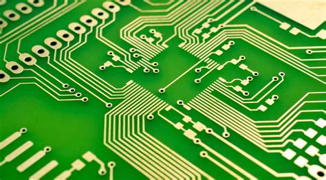
2. Imaging and Photolithography
The photolithography process transfers the circuit pattern onto the PCB using a photoresist. Precision requirements include:
- Alignment Accuracy: Misalignment between layers in multi-layer PCBs must be minimized (typically < 25 µm).
- Line Width and Spacing: Modern PCBs require trace widths as small as 25 µm (1 mil) or less, with tight tolerances (±10%).
- Resolution of Photoresist: High-resolution photoresists ensure sharp edges and prevent undercutting during etching.
3. Etching Process
Etching removes unwanted copper to form the conductive traces. Precision considerations include:
- Etch Factor: The ratio of vertical to lateral etching affects trace geometry. A high etch factor ensures minimal undercutting.
- Uniformity: Uneven etching can lead to open or short circuits.
- Over-Etching Prevention: Excessive etching can reduce trace width beyond acceptable limits.
4. Drilling and Hole Formation
Mechanical and laser drilling create vias and through-holes for interconnections. Key precision requirements:
- Hole Diameter Tolerance: Typically ±50 µm for standard PCBs, but ±25 µm or better for high-density designs.
- Positional Accuracy: Drilled holes must align precisely with pad centers (misalignment < 25 µm).
- Aspect Ratio: The ratio of hole depth to diameter affects plating quality (standard aspect ratio: 10:1; advanced PCBs may reach 20:1).
5. Plating (Through-Hole and Surface Plating)
Electroplating deposits copper inside holes and on surfaces to ensure conductivity. Precision factors include:
- Plating Thickness Uniformity: Typically 25-30 µm for through-holes, with ±5% tolerance.
- Copper Distribution: Uneven plating can cause weak interconnects or impedance mismatches.
- Surface Smoothness: Rough plating can lead to signal loss in high-frequency circuits.
6. Solder Mask Application
The solder mask insulates and protects the PCB. Precision requirements:
- Registration Accuracy: Misalignment can expose copper or cover pads, affecting solderability.
- Thickness Control: Too thin, and insulation fails; too thick, and component placement is hindered.
- Opening Size for Pads: Must match component lead dimensions precisely (±20 µm).
7. Surface Finish
The final surface treatment (e.g., HASL, ENIG, OSP) impacts solderability and reliability. Key precision aspects:
- Thickness Control: For ENIG, gold thickness (0.05-0.1 µm) and nickel (3-6 µm) must be tightly controlled.
- Flatness: Uneven surfaces (e.g., HASL) can cause poor solder joints in fine-pitch components.
8. Electrical Testing and Inspection
Automated optical inspection (AOI) and electrical testing verify precision:
- Impedance Control: High-speed PCBs require impedance tolerances of ±10%.
- Continuity and Isolation Testing: Ensures no open or short circuits exist.
Conclusion
Precision in PCB manufacturing is critical for performance, reliability, and miniaturization. As technology advances, tolerances become tighter, requiring advanced equipment and process control. Manufacturers must continuously improve techniques to meet the growing demands of modern electronics.