Precision Strategies for Reliable Fine Pitch PCB Assembly Manufacturing

Key Takeaways
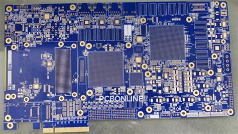
Achieving reliable PCB assembly in fine pitch applications demands a strategic approach that integrates precision engineering with rigorous quality protocols. Central to success is optimizing soldering processes—particularly for PCBA involving components with pitches below 0.5mm. Techniques such as laser reflow soldering and nitrogen-assisted environments minimize thermal stress while ensuring consistent joint formation. Equally critical is component alignment in densely packed layouts, where automated optical alignment systems reduce placement errors to sub-micron levels.
Advanced inspection methodologies, including 3D automated optical inspection (AOI) and X-ray tomography, play a pivotal role in identifying defects like solder bridging or voids, which are magnified in high-density designs. Material selection further influences outcomes, with low-CTE substrates and high-tg laminates mitigating warpage risks during thermal cycling. For handling delicate components, vacuum-assisted pick-and-place systems paired with anti-static protocols preserve integrity throughout the PCB assembly workflow.
Finally, integrating real-time thermal profiling ensures stable heat distribution across compact boards, preventing localized overheating in PCBA microcomponents. By harmonizing these elements, manufacturers can elevate yield rates while maintaining the reliability required for cutting-edge electronics.
Fine Pitch Soldering Optimization
Achieving reliable connections in fine pitch PCB assembly demands meticulous control over solder application and thermal management. Critical parameters such as solder paste deposition thickness and reflow temperature profiles directly influence joint integrity, especially with component leads spaced below 0.5mm. Modern PCBA workflows leverage laser-cut stencils with apertures under 100µm to ensure precise paste transfer, while nitrogen-assisted reflow ovens minimize oxidation risks during high-temperature cycles.
A common challenge in fine pitch soldering is preventing bridging or cold joints—defects that compromise electrical performance in high-density layouts. To mitigate these risks, manufacturers employ automated optical inspection (AOI) systems with 3D solder paste measurement capabilities, paired with real-time thermal profiling to validate process consistency. For ultra-fine components like 0.3mm-pitch BGAs, PCB assembly specialists often integrate vacuum-assisted pick-and-place systems to maintain alignment accuracy before reflow.
Advanced PCBA facilities now adopt adaptive soldering algorithms that dynamically adjust heating rates based on component thermal mass variations, ensuring uniform intermetallic bond formation. This approach not only reduces void formation but also enhances long-term reliability in mission-critical applications such as medical devices or aerospace electronics.
Component Alignment in Dense PCBs
Achieving precise component alignment in dense PCB assembly requires a combination of advanced equipment and process optimization. As electronic designs shrink, placement accuracy becomes critical to avoid bridging, open circuits, or misaligned connections. Modern PCBA workflows leverage automated optical alignment systems (AOAs) with micron-level precision, which use vision-guided robotics to position components as small as 01005 packages.
Key challenges include managing thermal drift during soldering and compensating for substrate warping in high-density layouts. To address these, manufacturers often employ:
| Technique | Purpose | Tolerance Range |
|---|---|---|
| Vision-Based Fiducials | Reference point calibration | ±5 µm |
| Laser-Assisted Placement | Real-time positional feedback | ±3 µm |
| Warpage Compensation | Adjust for board deformation | ±8 µm |
Additionally, stencil design and solder paste viscosity are optimized to prevent component shifting during reflow. For fine-pitch PCBA, using no-clean fluxes with controlled slump characteristics ensures minimal post-placement movement. Advanced inspection protocols, such as 3D solder paste inspection (SPI), further validate alignment integrity before reflow, reducing rework rates by up to 40% in complex assemblies.
Advanced PCB Assembly Inspection
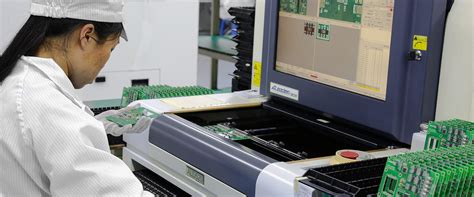
As component densities increase in modern electronics, PCB assembly processes demand inspection systems capable of detecting micron-level defects. Automated optical inspection (AOI) remains a cornerstone for verifying PCBA quality, employing high-resolution cameras and machine learning algorithms to identify solder bridging, misaligned components, or insufficient solder paste deposition. For ultra-fine pitch applications, X-ray inspection becomes indispensable, revealing hidden defects in ball grid arrays (BGAs) or under components with pitches below 0.4mm. Advanced systems now integrate 3D solder joint profiling to measure fillet heights and void percentages, critical for ensuring long-term reliability in high-density designs.
To maintain consistency, manufacturers are adopting statistical process control (SPC) tools that correlate inspection data with PCB assembly parameters, enabling real-time adjustments to stencil printing or reflow profiles. Infrared thermography further complements these methods by mapping thermal gradients during testing, identifying potential hotspots in tightly packed layouts. As PCBA complexity grows, hybrid inspection workflows combining AOI, X-ray, and functional testing have become essential for achieving defect rates below 50ppm in mission-critical applications. These layered approaches not only safeguard against assembly flaws but also provide traceable quality metrics for compliance with automotive or aerospace standards.
High-Density PCB Material Choices
Selecting appropriate materials is critical for ensuring reliability in fine pitch PCB assembly, where component density and thermal demands push conventional substrates to their limits. High-frequency applications often require specialized laminates like Rogers RO4000® series or polyimide-based substrates, which offer superior thermal stability and controlled dielectric constants to minimize signal loss. For PCBA designs involving ultra-fine traces (< 3 mil), low-profile copper foils (½ oz or ⅓ oz) paired with laser-drillable dielectrics reduce the risk of via wall roughness, enhancing signal integrity in high-speed circuits.
Tip: Always validate material compatibility with your soldering profile—some high-Tg FR-4 variants may require adjusted reflow parameters to prevent delamination during PCB assembly.
In thermally challenging environments, ceramic-filled prepregs or metal-core substrates (e.g., aluminum-clad PCBs) help dissipate heat from densely packed components. For solder mask selection, liquid photoimageable (LPI) solder masks provide precise coverage over microvias and fine-pitch pads, reducing solder bridging risks. When prioritizing electrical performance, consider hybrid stack-ups combining low-Dk materials for critical signal layers with cost-effective FR-4 for internal planes. This balanced approach optimizes both functionality and manufacturability in high-density PCBA workflows.
Fine Pitch PCB Handling Solutions
Effective handling of fine-pitch PCBs during PCB assembly requires specialized solutions to mitigate risks associated with high-density designs. Component fragility and micro-scale solder joints demand precision at every stage, from storage to placement. Automated systems equipped with vacuum grippers or electrostatic discharge (ESD)-safe nozzles are critical for maintaining component integrity, particularly when managing 0.4mm pitch or smaller devices.
To prevent warping or misalignment, manufacturers often employ anti-static trays and customized carriers designed to stabilize boards during transport through PCBA production lines. Advanced handling systems integrate real-time environmental monitoring to regulate humidity and temperature, which are pivotal for preserving solder paste viscosity and preventing oxidation.
For ultra-fine pitch components, robotic pick-and-place machines with vision-guided alignment ensure sub-micron accuracy, reducing placement errors that could compromise electrical connections. Additionally, anti-vibration workstations and low-inertia conveyors minimize mechanical stress during transit. These protocols not only enhance yield rates but also align with stringent quality standards required for high-reliability applications, such as medical devices or aerospace electronics.
By combining robust handling infrastructure with process automation, PCB assembly teams can address the unique challenges of fine-pitch designs while maintaining scalability and repeatability across production batches.

Thermal Solutions for Compact PCBs
Effective thermal management is critical in PCB assembly processes involving high-density designs, where component miniaturization intensifies heat dissipation challenges. Compact layouts in modern PCBA demand tailored strategies to prevent thermal stress, which can compromise solder joint integrity and component longevity. One approach involves selecting substrates with high thermal conductivity, such as metal-core or ceramic-filled laminates, to enhance heat transfer away from sensitive microcomponents.
Advanced thermal via arrays play a dual role: they improve electrical connectivity while channeling heat to inner copper layers or external heatsinks. For ultra-fine pitch applications, laser-drilled microvias enable precise heat redistribution without occupying valuable routing space. Integrating thermally conductive underfills or epoxy materials further stabilizes PCB assembly by reducing mechanical strain caused by temperature fluctuations.
Automated thermal simulation tools are now indispensable in prototyping, allowing engineers to model heat flow and identify hotspots before manufacturing. Post-assembly, infrared inspection systems validate thermal performance, ensuring even heat distribution across densely packed circuits. This proactive alignment of design and validation steps in PCBA workflows minimizes rework and sustains yield rates in mission-critical electronics.
By balancing material innovation, structural optimization, and rigorous testing, manufacturers achieve reliable thermal solutions that meet the demands of next-generation compact PCBs.
Maximizing PCB Assembly Yield
Achieving high yield in PCB assembly requires meticulous attention to process controls, material compatibility, and defect prevention strategies. At the core of PCBA optimization lies the synchronization of soldering profiles with component thermal requirements, particularly for fine-pitch devices where even minor deviations can lead to bridging or cold joints. Implementing statistical process control (SPC) enables real-time monitoring of critical parameters such as reflow oven temperature gradients and solder paste deposition accuracy, ensuring consistency across production batches.
Equally critical is the integration of automated optical inspection (AOI) and X-ray imaging to detect micro-scale defects in densely packed layouts. These systems identify misaligned components, insufficient solder joints, or microvoids that traditional visual checks might overlook. For high-density PCBA, selecting laminates with low coefficient of thermal expansion (CTE) minimizes warping during thermal cycling, directly improving assembly reliability.
Handling and storage protocols also play a pivotal role. Moisture-sensitive components, common in fine-pitch designs, demand controlled environments to prevent popcorning during reflow. Pairing humidity-sensitive packaging with nitrogen-rich reflow atmospheres further reduces oxidation risks. By aligning these strategies with design-for-manufacturability (DFM) principles, manufacturers can systematically address yield-limiting factors while maintaining scalability for complex PCB assembly projects.
PCB Microcomponent Quality Control
Ensuring the reliability of PCB assembly in fine-pitch applications demands rigorous quality control protocols for microcomponents. Critical path inspection begins with verifying component specifications, including dimensional accuracy and solderability, using automated optical inspection (AOI) and 3D X-ray systems. These tools detect submicron defects in PCBA, such as tombstoning or skewed placements, which are particularly challenging in high-density layouts.
Material integrity plays a pivotal role—microcomponents require precise storage conditions to prevent oxidation or moisture absorption, both of which compromise solder joint reliability. Advanced testing methods, like shear strength analysis and cross-sectional imaging, validate the mechanical and electrical bonds formed during reflow soldering. For PCB assembly lines, implementing real-time monitoring systems ensures process consistency, flagging deviations in parameters like temperature profiles or placement pressure.
A proactive approach involves correlating inspection data with yield metrics to identify recurring failure modes. For instance, deviations in solder paste volume, often traced to stencil wear, can be preemptively addressed through predictive maintenance schedules. By integrating statistical process control (SPC) into PCBA workflows, manufacturers achieve tighter tolerances while minimizing rework cycles—a necessity for maintaining profitability in precision-driven applications.
Conclusion
In high-density electronic manufacturing, achieving consistent reliability in PCB assembly demands a meticulous integration of design, process control, and validation. The strategies discussed—from optimizing soldering techniques to implementing rigorous inspection protocols—highlight the necessity of balancing precision with scalability in PCBA workflows. As component miniaturization accelerates, manufacturers must prioritize advanced alignment systems and thermal management solutions to mitigate risks such as solder bridging or component displacement.
A successful fine-pitch PCB assembly strategy hinges on three pillars: material compatibility, process repeatability, and real-time quality assurance. By leveraging automated optical inspection (AOI) and X-ray testing, defects in densely packed layouts can be identified early, preserving yield rates. Furthermore, adopting anti-static handling protocols ensures the integrity of microcomponents throughout the PCBA lifecycle.
Ultimately, the convergence of these methodologies not only enhances product longevity but also future-proofs manufacturing lines against evolving industry demands. For engineers and assemblers, staying ahead requires continuous refinement of both technical expertise and equipment capabilities, ensuring that every PCB assembly meets the exacting standards of modern high-performance applications.
Frequently Asked Questions
What are the primary challenges in fine pitch pcb assembly?
Achieving reliable connections in high-density PCBA requires precise control over solder paste deposition and component placement accuracy. Even minor deviations can lead to bridging or open circuits, particularly with components featuring pitches below 0.4mm.
How does soldering process optimization improve yield in pcb assembly?
Advanced techniques like laser soldering and nitrogen-reflow environments minimize oxidation and ensure consistent joint formation. Pairing these methods with 3D automated optical inspection (AOI) helps detect defects early, reducing rework costs.
What role do materials play in reliable PCBA for high-density designs?
Low-CTE substrates and high-Tg laminates mitigate thermal stress, while halogen-free solder masks enhance durability. Selecting materials compatible with microcomponent soldering is critical to prevent warping during reflow cycles.
Can traditional inspection methods suffice for fine pitch pcb assembly?
Standard 2D AOI systems often miss planar defects in ultra-dense layouts. Implementing X-ray inspection or 3D SPI (solder paste inspection) ensures better detection of hidden voids or misalignments in miniaturized PCBA configurations.
How do environmental factors impact fine pitch assembly reliability?
Humidity and temperature fluctuations during storage can degrade solder paste performance. Controlled storage conditions and moisture-sensitive component baking protocols are essential to maintain interconnection integrity in humidity-prone environments.
Explore Custom Solutions for Your Project
For tailored strategies in high-density PCB assembly, please click here to consult our engineering team at https://www.andwinpcb.com/pcb-assembly/.