Precision Techniques for Reliable PC Board Assembly
Key Takeaways
Effective PCB assembly relies on mastering precision soldering techniques, such as reflow and wave soldering, to ensure robust electrical connections. Equally critical is strategic component placement, which minimizes signal interference and optimizes thermal management in PCBA workflows. Implementing rigorous quality control protocols—including automated optical inspection (AOI) and X-ray testing—helps identify defects early, enhancing the durability of assembled boards.
To avoid common errors, manufacturers must prioritize design-for-manufacturability (DFM) principles, ensuring components align with PCB assembly tolerances. Advanced strategies, such as 3D solder paste inspection and thermal profiling, further refine reliability in PCBA processes. Transitioning between these steps requires seamless coordination between design and production teams, supported by real-time data analytics.
Finally, integrating environmental stress testing and functional verification during post-assembly phases ensures long-term performance. By balancing technical precision with systematic oversight, electronics manufacturers can achieve consistent results while reducing rework costs. These practices form the foundation of modern PCB assembly, bridging innovation with operational efficiency.
Precision Soldering Methods for PCB Assembly
Achieving reliable PCBA requires meticulous attention to soldering techniques, as even minor inconsistencies can compromise electrical connectivity or mechanical stability. Modern PCB assembly processes employ advanced methods such as reflow soldering and selective soldering, each optimized for specific component types and board complexities. For surface-mount devices (SMDs), reflow soldering uses precisely controlled temperature profiles to melt solder paste uniformly, ensuring strong intermetallic bonds without thermal damage. Through-hole components, however, often demand wave soldering or hand-soldering with temperature-regulated irons to maintain joint integrity.
Critical parameters in precision soldering include:
| Factor | Optimal Range | Impact on Quality |
|---|---|---|
| Solder Alloy Composition | SAC305 (Sn96.5/Ag3/Cu0.5) | Enhances thermal fatigue resistance |
| Peak Temperature | 240–250°C (reflow) | Prevents component warping |
| Cooling Rate | 2–4°C/sec | Reduces solder joint brittleness |
Automated optical inspection (AOI) systems validate solder joint quality by detecting defects like bridging or cold joints, while X-ray inspection ensures hidden connections in ball grid arrays (BGAs) meet specifications. To minimize human error, manufacturers integrate closed-loop feedback systems that adjust soldering parameters in real time based on sensor data. For high-density PCBA, nitrogen-assisted soldering environments reduce oxidation, improving wetting behavior and joint reliability.
Technician training remains vital, particularly for hybrid assemblies combining SMDs and through-hole parts. Certifications such as IPC-A-610 and J-STD-001 establish standardized criteria for acceptability, ensuring consistency across production batches. By combining advanced equipment with rigorous process controls, PCB assembly achieves the precision required for today’s high-performance electronics.
Component Placement Strategies in Electronics Manufacturing
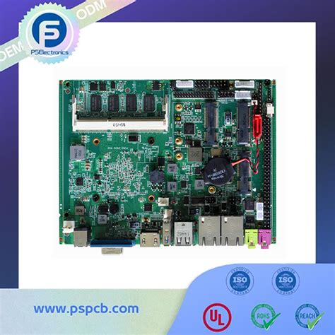
Effective PCB assembly relies on precise component placement to balance functionality, thermal management, and manufacturability. Modern surface-mount technology (SMT) systems leverage automated pick-and-place machines to achieve micron-level accuracy, reducing human error while accommodating miniaturized components. Critical considerations include thermal dissipation patterns for heat-sensitive parts, proper spacing to avoid electromagnetic interference, and alignment with PCBA design guidelines to ensure solder joint integrity.
Strategies often prioritize grouping components by function or power requirements, streamlining signal pathways and simplifying testing protocols. For mixed-technology boards, combining through-hole components with SMT parts demands meticulous planning to avoid reflow oven conflicts. Advanced PCB assembly workflows integrate real-time optical inspection (AOI) to verify placement accuracy before soldering, minimizing rework.
Additionally, designers must account for mechanical stresses during operation, using anti-vibration layouts or reinforced mounting for heavy components. By aligning placement strategies with Design for Manufacturing (DFM) principles, engineers optimize both production efficiency and end-product reliability. This systematic approach not only accelerates PCBA cycles but also lays the groundwork for rigorous quality control in subsequent stages.
Quality Control Protocols for Durable PCB Assembly
Implementing rigorous quality control protocols is critical for ensuring the reliability and longevity of PCB assembly processes. Modern PCBA manufacturing relies on multi-stage inspections, beginning with automated optical inspection (AOI) systems to detect soldering defects, misaligned components, or insufficient solder joints. X-ray inspection further examines hidden connections in ball grid array (BGA) packages, ensuring internal integrity.
Tip: Incorporate environmental stress testing, such as thermal cycling, to simulate real-world operating conditions and identify potential failure points before final product delivery.
Statistical process control (SPC) tools track production metrics like solder paste volume and reflow oven temperatures, maintaining consistency across batches. For high-reliability applications, cross-sectional analysis validates solder joint quality, while functional testing confirms electrical performance against design specifications.
Adherence to IPC-A-610 standards ensures compliance with industry benchmarks for acceptable workmanship. Documentation practices, including traceability logs for components and materials, streamline root-cause analysis if field failures occur. By integrating these protocols, manufacturers minimize rework costs and deliver durable PCB assemblies that meet stringent performance requirements.
Optimizing Performance Through PCB Assembly Techniques
Achieving peak performance in PCB assembly requires meticulous attention to both design and execution. Central to this process is the alignment of thermal management strategies with signal integrity considerations. By leveraging advanced PCBA methodologies, manufacturers can minimize impedance mismatches and reduce electromagnetic interference (EMI), which are critical for high-frequency applications. For instance, precise control over solder paste deposition—using stencil printing techniques with laser-cut apertures—ensures consistent joint formation, directly impacting circuit reliability.
Another key factor is the integration of design for manufacturability (DFM) principles early in the development cycle. This involves optimizing component layouts to prevent heat concentration zones and ensuring adequate spacing for automated pick-and-place systems. PCB assembly workflows benefit from real-time monitoring tools, such as automated optical inspection (AOI), which detect soldering defects like bridging or insufficient fillets before final testing.
Material selection also plays a pivotal role. High-performance substrates with low dielectric loss and robust PCBA-compatible finishes (e.g., ENIG or HASL) enhance durability in harsh environments. Additionally, implementing conformal coating processes shields sensitive components from moisture and contaminants, extending operational lifespans. By balancing these technical considerations with rigorous testing protocols—such as in-circuit testing (ICT) and functional validation—manufacturers can systematically elevate both the efficiency and reliability of assembled boards.
Avoiding Common Errors in PC Board Component Placement
Accurate component placement is critical in PCB assembly to prevent functional failures and ensure long-term reliability. One frequent error involves misalignment of surface-mount devices (SMDs), which can lead to poor solder joints or short circuits. To mitigate this, manufacturers rely on automated optical inspection (AOI) systems to verify alignment before soldering. Another common issue stems from incorrect polarity or orientation of components like capacitors or diodes. Implementing pick-and-place machines with vision-guided calibration significantly reduces such errors by ensuring precise positioning according to design specifications.
Thermal management is another overlooked factor. Placing heat-sensitive components near high-power devices without adequate spacing can cause thermal stress, compromising performance. Adhering to thermal relief patterns in the design phase and maintaining proper airflow during PCBA helps address this. Additionally, improper handling of electrostatic discharge (ESD)-sensitive parts during placement can degrade their functionality. Utilizing grounded workstations and anti-static tools is essential for safeguarding components.
Finally, neglecting to validate component footprints against the board layout often results in mechanical mismatches. Cross-referencing bill of materials (BOM) data with CAD models ensures compatibility. By integrating these practices, manufacturers can minimize rework, enhance yield rates, and deliver electronics manufacturing solutions that meet stringent quality benchmarks.
Advanced Strategies for Reliable Electronics Assembly
Modern PCB assembly demands a systematic approach to balance speed, accuracy, and durability. One critical advancement involves integrating predictive analytics into PCBA workflows, enabling real-time monitoring of solder joint integrity and component alignment. By leveraging machine learning algorithms, manufacturers can identify potential defects—such as cold solder joints or misaligned ICs—before they compromise product performance.
Another key strategy focuses on thermal management during assembly. High-density PCB assembly often generates localized heat, which can warp substrates or weaken connections. Implementing controlled reflow profiles and selecting thermally stable materials, such as polyimide-based laminates, ensures consistent performance under stress. Additionally, automated optical inspection (AOI) systems paired with X-ray imaging provide multi-layered quality assurance, detecting hidden flaws like voids in ball grid arrays (BGAs).
For mission-critical applications, adopting failure mode and effects analysis (FMEA) during PCBA design phases minimizes risks. This proactive method evaluates how component placement, trace routing, and material choices interact under operational extremes. Combining this with design-for-manufacturability (DFM) principles reduces rework rates by up to 40%, aligning with stringent industry standards.
Finally, fostering collaboration between design engineers and assembly technicians ensures seamless translation of schematics into physical boards. This synergy optimizes PCB assembly outcomes, balancing technical precision with scalable production workflows.
Ensuring Longevity in PCB Manufacturing Processes
Achieving long-term reliability in PCB assembly requires integrating robust design principles with meticulous manufacturing practices. A critical starting point is selecting materials that withstand environmental stressors, such as high-Tg substrates for thermal resilience and immersion silver or gold finishes to combat oxidation. Modern PCBA workflows emphasize controlled thermal profiles during soldering to prevent micro-cracks, ensuring joints remain intact under mechanical or thermal strain.
Proactive measures like conformal coating application shield components from moisture, dust, and chemical exposure—common culprits in premature failure. Advanced manufacturers also implement automated optical inspection (AOI) systems to detect latent defects, such as insufficient solder paste or misaligned components, before boards enter high-stress environments. For applications demanding extreme durability, accelerated life testing simulates years of operational wear in compressed cycles, validating design choices under realistic conditions.
Balancing performance with longevity involves optimizing trace widths and spacing to minimize electromigration risks while maintaining signal integrity. Additionally, incorporating PCB assembly best practices—like avoiding tombstoning through symmetric pad designs—reduces rework needs and preserves structural integrity. By aligning material science, process engineering, and rigorous testing, manufacturers ensure PCBA products deliver consistent performance across their intended lifespan.
Expert Tips for Precision Assembly and Testing
Achieving consistent results in PCB assembly requires a combination of technical expertise and systematic validation processes. Begin by verifying thermal profiles for reflow soldering to prevent component stress, ensuring temperatures align with material specifications. Use automated optical inspection (AOI) systems to detect micro-scale defects like solder bridges or misaligned components, which are critical for high-density PCBA designs. For sensitive components, employ vacuum-assisted pick-and-place machines to minimize positional errors during mounting.
Transitioning to testing phases, integrate in-circuit testing (ICT) to validate electrical connectivity and functional testing (FCT) to simulate real-world operating conditions. Implement boundary scan testing for complex circuits, enabling early identification of signal integrity issues. Maintain traceability through barcode tracking systems, linking each PCB assembly to its quality metrics for rapid troubleshooting. Finally, conduct accelerated life testing under controlled thermal and vibrational loads to assess long-term reliability. By harmonizing these methods, manufacturers can reduce rework rates while meeting stringent performance benchmarks in electronics manufacturing.
Conclusion
Effective PCB assembly hinges on integrating precision techniques with rigorous quality assurance to deliver durable and high-performing electronic systems. By prioritizing accurate component placement and controlled soldering processes, manufacturers can minimize defects and enhance the reliability of PCBA outcomes. Advanced strategies, such as automated optical inspection and thermal profiling, further ensure that each assembly meets stringent performance benchmarks while mitigating risks like solder bridging or misalignment.
A systematic approach to PCB assembly also demands continuous refinement of testing protocols, from functional verification to environmental stress screening. These steps not only validate the integrity of the PCBA but also extend its operational lifespan in demanding applications. As the electronics industry evolves, adopting adaptive manufacturing workflows and leveraging data-driven insights will remain critical for maintaining competitiveness. Ultimately, the convergence of technical expertise, cutting-edge tools, and proactive error prevention defines success in modern PCB assembly, enabling manufacturers to meet both current demands and future challenges in electronics production.
Frequently Asked Questions
What distinguishes basic PCB assembly from advanced PCBA processes?
PCB assembly refers to the foundational process of populating a bare board with components, while PCBA (Printed Circuit Board Assembly) encompasses the complete cycle—including soldering, testing, and quality validation. Advanced PCBA integrates automated optical inspection (AOI) and X-ray verification for mission-critical applications.
How does temperature control affect soldering reliability?
Precise temperature profiling ensures proper solder joint formation without damaging components. Variations exceeding ±5°C may cause cold joints or delamination, compromising PCB assembly longevity. Industrial-grade reflow ovens maintain tolerances within 1.5°C for consistent results.
What are common pitfalls in component placement accuracy?
Misaligned ICs or reversed polarities often stem from insufficient fiducial marker calibration. Modern PCBA lines use machine vision systems achieving ±0.025mm placement precision, reducing human error by 89% in high-density designs.
Why is conformal coating critical for durable assemblies?
This protective layer shields against moisture ingress and chemical corrosion, extending operational lifespans by 3–5× in harsh environments. Post-coating inspections verify uniform application without obstructing test points or connectors.
Ready to Optimize Your PCB Assembly Workflow?
For tailored PCBA solutions combining ISO-certified manufacturing with DFM (Design for Manufacturability) analysis, please click here to consult our engineering team.


