Precision Techniques in Modern PBA Printed Board Assembly

Key Takeaways
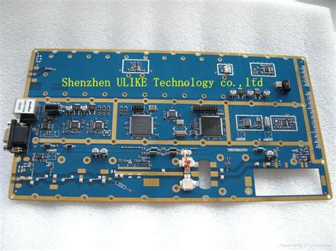
Modern PCB assembly (PCBA) processes rely on precision techniques to meet the demands of high-reliability industries like aerospace, medical, and consumer electronics. Central to these advancements are laser soldering and micro-component placement systems, which enable sub-millimeter accuracy for densely packed circuits. Automated quality control (QC) tools, such as automated optical inspection (AOI) and X-ray testing, have become indispensable for detecting defects in real time, ensuring compliance with stringent industry standards.
| Technique | Application | Key Benefit |
|---|---|---|
| Laser Soldering | High-density interconnects | Minimizes thermal stress |
| AOI Systems | Surface-mount validation | Rapid defect identification |
| X-ray Inspection | BGA/QFN component analysis | Non-destructive layer scrutiny |
In aerospace PCBA, conformal coating and vibration-resistant designs are prioritized to withstand extreme environments. Medical electronics demand biocompatible materials and sterilization-compatible assemblies, while consumer devices focus on miniaturization and cost-effective scalability. By integrating these methodologies, manufacturers achieve reliability across production cycles, balancing performance with regulatory compliance. Transitioning between design, assembly, and QC phases requires seamless coordination—a hallmark of next-gen PCB assembly workflows.
Laser Soldering in PCB Manufacturing
Laser soldering has emerged as a precision-critical technique in modern PCB assembly, enabling manufacturers to address the growing demand for miniaturized and high-density PCBA designs. Unlike traditional reflow methods, laser systems deliver localized heat through focused beams, minimizing thermal stress on adjacent components—a vital advantage for heat-sensitive materials in aerospace or medical devices. This method ensures consistent joint formation, even with micro-scale solder pads, by dynamically adjusting parameters like power and pulse duration.
The integration of automated optical inspection (AOI) systems further enhances process reliability, allowing real-time monitoring of solder joint quality. For consumer electronics, where component density and lead spacing continue to shrink, laser soldering reduces defects such as bridging or cold joints. Additionally, its non-contact nature eliminates mechanical wear, making it ideal for high-mix, low-volume PCBA production.
By combining flexibility with repeatability, this technology supports the shift toward Industry 4.0-compliant manufacturing lines. Engineers can program laser paths for complex layouts, ensuring alignment with design tolerances down to ±10µm. As industries prioritize reliability in harsh environments, laser soldering remains a cornerstone of advanced PCB assembly strategies.
Micro-Component Placement Strategies
Achieving precision in PCB assembly demands advanced strategies for placing miniature components, particularly as devices shrink and functionality expands. Modern PCBA workflows leverage high-speed pick-and-place systems equipped with vision-guided robotics, enabling accurate positioning of components as small as 01005 metric packages (0.4 mm × 0.2 mm). These systems utilize real-time feedback mechanisms to compensate for thermal expansion or mechanical drift, ensuring placement tolerances below 50 microns.
Tip: For high-density designs, consider integrating 3D solder paste inspection (SPI) before component placement to mitigate defects caused by uneven paste deposition.
A critical challenge in micro-component placement lies in managing component warping and static discharge, especially in humidity-sensitive environments. Aerospace and medical PCBA applications often employ nitrogen-controlled chambers to stabilize ambient conditions during placement. Additionally, tandem feeding systems allow simultaneous handling of mixed component sizes, reducing cycle times in complex assemblies.
"Precision placement isn’t just about speed—it’s about harmonizing mechanical accuracy with material science," notes a senior process engineer at a leading electronics manufacturer.
To ensure repeatability, manufacturers are adopting machine learning algorithms that analyze historical placement data to predict and correct misalignments. This approach is particularly effective in PCB assembly lines producing wearable medical devices, where component density exceeds 200 parts per square inch. By balancing speed, precision, and environmental controls, modern strategies in micro-component placement are redefining reliability standards across industries.
Automated QC for PBA Reliability
Modern PCB assembly processes demand rigorous quality control (QC) frameworks to meet the exacting standards of industries like aerospace and medical electronics. Automated QC systems now integrate advanced technologies such as automated optical inspection (AOI) and X-ray tomography to detect microscopic defects in PCBA units, including solder joint irregularities, misaligned components, and trace fractures. These systems leverage machine learning algorithms to analyze thousands of data points per board, identifying anomalies with sub-micron precision. For instance, 3D SPI (solder paste inspection) tools map solder paste deposition accuracy before reflow, minimizing post-assembly rework.
In high-reliability applications, in-circuit testing (ICT) and functional testing validate electrical performance under simulated operational conditions. Automated systems also track environmental variables like temperature and humidity during PCB assembly, ensuring compliance with industry-specific certifications. By reducing human intervention, these QC protocols achieve defect rates below 50 ppm in consumer electronics PCBA lines while maintaining traceability through blockchain-enabled data logging. Transitioning seamlessly from micro-component placement strategies, automated QC bridges precision manufacturing with end-product dependability, setting the stage for innovations in aerospace and medical device reliability discussed in subsequent sections.
Aerospace PBA Manufacturing Trends
The aerospace sector demands PCB assembly processes that prioritize extreme reliability under harsh operational conditions. Thermal cycling, vibration resistance, and miniaturization drive innovation in PCBA design, with manufacturers adopting advanced materials like polyimide substrates and ceramic-filled laminates. To meet stringent MIL-PRF-31032 standards, laser-assisted soldering ensures precision joints for high-density interconnects, while robotic pick-and-place systems achieve micron-level accuracy for components as small as 01005 packages.
Recent advancements integrate in-process inspection via automated optical systems, which validate solder joint integrity and component alignment in real time. This reduces latent defects in avionics and satellite communication systems, where failure tolerance approaches zero. Additionally, additive manufacturing techniques now support rapid prototyping of conformal-shielded PCBA units, critical for reducing electromagnetic interference in next-gen aircraft.
As aerospace applications increasingly adopt modular architectures, flex-rigid hybrid boards and embedded passive components are reshaping PCB assembly workflows. These trends not only enhance durability in extreme environments but also align with weight reduction goals for fuel-efficient airframes. By merging cutting-edge PCBA technologies with rigorous testing protocols, manufacturers ensure mission-critical systems operate flawlessly across decades-long service lifecycles.
Medical Electronics Assembly Innovations
Advancements in PCB assembly for medical devices demand sub-micron accuracy to meet stringent regulatory standards. Modern PCBA processes now integrate laser-assisted soldering and 3D automated optical inspection (AOI), enabling defect rates below 0.01% in critical applications like implantable devices and diagnostic equipment. For instance, high-density interconnect (HDI) boards with micro-BGA components are essential for miniaturized pacemakers, where reliability directly impacts patient safety.
To ensure compliance with ISO 13485 and FDA guidelines, manufacturers deploy real-time thermal profiling during reflow soldering, preventing thermal stress on sensitive components. Additionally, traceability systems embedded in PCBA workflows track every solder joint and component placement, streamlining audits and recalls. Innovations such as flexible hybrid electronics (FHE) further support wearable medical sensors, combining rigid and flexible substrates for ergonomic designs.
Transitioning from aerospace or consumer electronics, medical PCB assembly prioritizes biocompatible materials and hermetic sealing techniques. This shift underscores the industry’s focus on merging precision PCBA methods with life-critical performance, ensuring devices operate flawlessly in environments ranging from operating rooms to home healthcare settings.
Consumer Electronics PBA Solutions
The consumer electronics sector demands PCB assembly processes that balance miniaturization, cost efficiency, and performance. As devices like smartphones, wearables, and smart home systems shrink in size but grow in functionality, PCBA manufacturers must integrate high-density interconnects and multi-layer board designs while maintaining signal integrity. Advanced surface-mount technology (SMT) enables precise placement of micro-components such as 01005 resistors and ultra-thin ICs, critical for compact designs. To address thermal challenges in tightly packed devices, engineers employ copper-core substrates and thermal interface materials, ensuring heat dissipation without compromising form factors.
Automated optical inspection (AOI) and X-ray testing have become indispensable in PCB assembly lines, catching defects like micro-cracks or solder bridging early in production. For high-volume consumer electronics, flexible manufacturing systems allow rapid reconfiguration between product batches, supporting fast time-to-market cycles. Emerging trends, such as foldable device architectures, further push PCBA innovation, requiring hybrid rigid-flex boards and laser-drilled vias for dynamic bending zones. By aligning with design-for-manufacturability (DFM) principles, manufacturers mitigate risks in mass production while meeting stringent reliability standards for everyday consumer use.
Ensuring PBA Reliability in Production
Achieving consistent reliability in PCB assembly requires a multi-layered approach to quality assurance, particularly in high-stakes industries like aerospace and medical devices. At the core of dependable PCBA manufacturing lies automated optical inspection (AOI) systems, which scan boards at micron-level precision to detect soldering defects, component misalignment, or trace irregularities. These systems work in tandem with X-ray inspection for hidden faults in ball grid arrays (BGAs) or underfill applications, ensuring even sub-surface connections meet stringent standards.
To maintain process stability, manufacturers implement statistical process control (SPC) tools that monitor variables such as solder paste deposition volume and reflow oven temperature profiles. This data-driven methodology minimizes deviations, a critical factor when producing PCB assemblies for environments with extreme thermal or vibrational stresses. Furthermore, environmental stress screening (ESS) subjects finished boards to accelerated aging tests—thermal cycling, humidity exposure, and mechanical shock—to simulate years of operational wear within controlled lab conditions.
The integration of traceability systems ensures every PCBA can be tracked through its lifecycle, linking production parameters to performance data. This closed-loop feedback mechanism allows engineers to refine assembly protocols iteratively, aligning with the precision demands outlined in earlier sections on aerospace and medical applications. By harmonizing advanced inspection technologies with rigorous testing protocols, manufacturers systematically eliminate failure points, delivering PCB assemblies that meet both functional specifications and long-term reliability expectations.
Modern PBA Assembly Techniques
At the core of contemporary PCB assembly lies the integration of advanced methodologies that balance precision with scalability. Laser soldering, for instance, has emerged as a cornerstone for high-density PCBA, enabling sub-millisecond heat application to minimize thermal stress on sensitive components. This technique is particularly vital in aerospace applications, where vibration resistance and thermal stability are non-negotiable.
Another critical aspect is the deployment of micro-component placement systems, which utilize vision-guided robotics to achieve placement accuracies under 10 microns. Such systems ensure seamless integration of 0201 or 01005 package components, a necessity for compact medical devices and wearables. Automated optical inspection (AOI) and X-ray computed tomography (XCT) further enhance PCB assembly reliability by detecting solder joint defects or misalignments invisible to the naked eye.
Transitioning toward Industry 4.0, smart factories now embed machine learning algorithms within PCBA workflows to predict equipment maintenance needs and optimize throughput. These innovations not only reduce human error but also align with stringent quality benchmarks in automotive and industrial electronics. By harmonizing cutting-edge tools with rigorous process controls, modern assembly techniques ensure that PCB assembly meets the exacting demands of next-generation technologies.
Conclusion
The evolution of PCB assembly (PCBA) reflects the growing demand for precision and reliability across industries such as aerospace, medical technology, and consumer electronics. Modern techniques like laser soldering and micro-component placement have redefined manufacturing standards, enabling the production of compact, high-performance assemblies capable of meeting stringent operational requirements. Automated quality control systems, integrated with advanced imaging and machine learning, now ensure near-flawless defect detection, minimizing risks in mission-critical applications.
As industries push toward miniaturization and higher functionality, PCBA processes must balance speed with meticulous accuracy. Innovations in thermal management and signal integrity optimization further underscore the importance of precision in high-density layouts. By leveraging these advancements, manufacturers can address the dual challenges of scalability and reliability, ensuring that printed board assemblies remain at the forefront of technological progress. The continued integration of intelligent automation and data-driven analytics promises to elevate PCB assembly to new heights, reinforcing its role as a cornerstone of modern electronics manufacturing.
Frequently Asked Questions
What distinguishes PCB assembly from PCBA in modern manufacturing?
PCB assembly refers to the process of populating a bare circuit board with components, while PCBA (Printed Circuit Board Assembly) denotes the completed board with all functional elements. Advanced techniques like laser soldering and automated optical inspection are now integral to both stages, ensuring micron-level precision.
How do aerospace applications influence PCBA design standards?
Aerospace PCB assemblies require hermetic sealing and vibration-resistant mounting to withstand extreme conditions. Manufacturers employ high-temperature laminates and conformal coatings, often integrating real-time thermal monitoring during PCBA to prevent failure in low-pressure environments.
What role does automation play in medical PCB assembly quality control?
Automated X-ray inspection (AXI) systems detect micro-solder voids in implantable device PCBAs, achieving <0.1% defect rates. Robotic pick-and-place machines handle 01005-sized components with 5µm accuracy, critical for patient monitoring systems where reliability impacts diagnostics.
Can consumer electronics PCB assembly balance speed and precision?
Yes. High-speed surface-mount technology (SMT) lines now place 80,000 components/hour with 3σ placement accuracy. Combined with AI-driven solder paste inspection, this enables mass production of 5G-enabled devices without compromising PCBA integrity.
Why is thermal management crucial in high-density PCB assemblies?
As components shrink below 0.4mm pitch, heat dissipation challenges grow. Techniques like embedded copper pillars and selective conformal coating maintain thermal thresholds below 85°C in ultra-compact PCBAs, preventing performance degradation in IoT edge devices.
Optimize Your Next Project with Expert PCB Assembly
For tailored solutions in aerospace-grade or high-density PCB assembly, please click here: https://www.andwinpcb.com/pcb-assembly/ to consult our engineering team about achieving MIL-STD-883 compliance or implementing zero-defect manufacturing protocols.


