Principles, Key Points, Methods, and Precautions for PCB Desoldering
Introduction
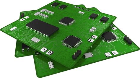
Printed Circuit Board (PCB) desoldering is a critical skill in electronics repair, rework, and component recycling. Proper desoldering techniques ensure component integrity, maintain PCB quality, and prevent damage to surrounding circuitry. This comprehensive guide covers the fundamental principles, essential work points, various methods, and important precautions for effective PCB desoldering.
I. Fundamental Principles of PCB Desoldering
1. Thermal Management Principle
Effective desoldering requires precise control of heat application. The thermal energy must be sufficient to melt the solder without damaging components or the PCB substrate. Different components and solder types require specific temperature ranges:
- Lead-based solder: 183-190°C (361-374°F)
- Lead-free solder: 217-227°C (423-441°F)
- Large components/ground planes: May require higher temperatures
2. Mechanical Stability Principle
Components and PCB pads must remain mechanically stable during desoldering. Excessive force can damage pads or lift traces. The process should minimize mechanical stress on both the component being removed and adjacent components.
3. Time Minimization Principle
Heat exposure time should be minimized to prevent:
- PCB delamination
- Component thermal damage
- Pad/trace lifting
- Solder mask degradation
4. Contamination Prevention Principle
Maintain cleanliness throughout the process to avoid:
- Solder splatter
- Flux residue buildup
- Foreign material introduction
II. Key Work Points in PCB Desoldering
1. Pre-Desoldering Preparation
- Component Identification: Determine component type (through-hole, SMD, BGA), package size, and pin count
- PCB Analysis: Identify board layers, ground/power planes, and heat-sensitive areas
- Solder Type Determination: Recognize whether lead-based or lead-free solder was used
- Tool Selection: Choose appropriate tools based on component and board characteristics
2. Workspace Setup
- ESD Protection: Use grounded mats and wrist straps for static-sensitive components
- Ventilation: Ensure proper fume extraction for solder/flux fumes
- Lighting: Provide adequate illumination for precise work
- Tool Organization: Arrange all necessary tools within easy reach
3. Component-Specific Considerations
- Through-Hole Components: Focus on complete solder removal from plated through-holes
- Surface Mount Devices (SMDs): Address multiple simultaneous solder joints
- Ball Grid Arrays (BGAs): Require specialized equipment and techniques
- Multi-pin Connectors: Need careful sequential desoldering
4. Post-Desoldering Procedures
- Pad Cleaning: Remove residual solder and flux
- Inspection: Verify pad and via integrity
- Preparation for Resoldering: Clean and tin pads if reusing the location
III. PCB Desoldering Methods
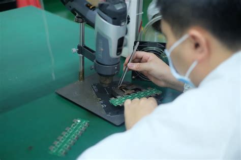
1. Manual Soldering Iron Techniques
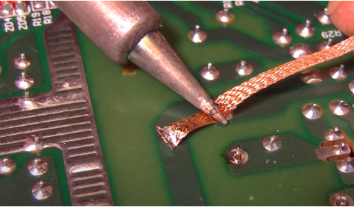
a) Solder Wick (Braiding)
- Process: Place copper braid over joint, apply iron to heat through braid
- Best For: Small components, touch-up work
- Advantages: Precise, low-cost
- Limitations: Slow for multiple pins, can leave residue
b) Solder Sucker (Vacuum Desoldering)
- Process: Melt solder, then use spring-loaded vacuum to remove
- Best For: Through-hole components
- Advantages: Fast for single joints
- Limitations: Can leave residual solder, requires coordination
2. Hot Air Rework Systems
- Process: Direct controlled hot air to component area to melt all joints simultaneously
- Best For: SMD components, multi-pin devices
- Advantages: Non-contact, good for dense layouts
- Limitations: Requires skill, can affect nearby components
3. Desoldering Stations
a) Vacuum Desoldering Stations
- Process: Combine heated tip with continuous vacuum
- Best For: High-volume through-hole work
- Advantages: Clean hole clearing, professional results
- Limitations: Expensive, requires maintenance
b) Hot Tweezers
- Process: Dual heated tips grasp SMD component ends
- Best For: Two-terminal SMDs (resistors, capacitors)
- Advantages: Precise component removal
- Limitations: Limited to small components
4. Specialized Methods
a) Infrared Rework
- Process: Use IR energy to heat component area
- Best For: BGA components, sensitive assemblies
- Advantages: Precise temperature control
- Limitations: High equipment cost
b) Chip Quik Low-Temperature Alloy
- Process: Add low-melting alloy to reduce overall joint temperature
- Best For: Heat-sensitive components
- Advantages: Protects components and PCB
- Limitations: Requires cleanup, additional materials
IV. Critical Precautions in PCB Desoldering
1. Thermal Damage Prevention
- Use the minimum effective temperature
- Limit dwell time (typically < 3-5 seconds per joint)
- For heat-sensitive components, consider:
- Heat sinks on component leads
- Thermal shields for adjacent components
- Pulsed heating rather than continuous application
2. Mechanical Stress Avoidance
- Never force components before solder is fully melted
- For multi-pin components, work systematically:
- Alternate between pins to prevent stress concentration
- Consider partial removal techniques for large components
- Use proper support for flexible PCBs during desoldering
3. PCB Protection Measures
- Be aware of pad adhesion strength (varies by PCB quality)
- Recognize when to use additional flux (improves heat transfer)
- Understand when to add fresh solder (improves thermal coupling)
- Know when to stop (if pads show signs of lifting)
4. Component-Specific Precautions
- Electrolytic Capacitors: Extremely heat-sensitive, remove quickly
- Plastic Connectors: Can melt with excessive heat
- BGAs: Require precise temperature profiling
- Fine-Pitch Components: High risk of pad damage
5. Health and Safety Considerations
- Always work in well-ventilated areas
- Use appropriate personal protective equipment:
- Safety glasses
- Heat-resistant gloves when needed
- ESD protection for sensitive components
- Be aware of lead exposure risks with lead-based solder
- Properly dispose of solder waste and used materials
V. Advanced Techniques and Troubleshooting
1. Dealing with Difficult Situations
- Corroded Joints: May require additional flux or mechanical agitation
- Plated Through-Hole Clearing: Sometimes needs multiple approaches
- Multi-layer Board Challenges: Require careful heat management
2. Common Problems and Solutions
- Lifted Pads: May require trace repair or alternative connection methods
- Component Damage: Often results from excessive force or heat
- Residual Solder: Can be addressed with different techniques or tools
3. Equipment Maintenance
- Regular tip cleaning and tinning for soldering irons
- Nozzle cleaning for hot air systems
- Filter replacement for vacuum systems
- Calibration checks for temperature-controlled equipment

VI. Best Practices for Professional Results
- Develop a Systematic Approach: Create and follow consistent procedures
- Master Multiple Techniques: Be proficient with various methods for different situations
- Document Your Work: Keep notes on successful techniques for specific components
- Continuous Learning: Stay updated on new materials and techniques
- Quality Focus: Prioritize PCB and component integrity over speed
Conclusion
Effective PCB desoldering requires understanding of thermal principles, mechanical considerations, and proper technique application. By following the outlined principles, key work points, method selections, and precautions, technicians can achieve successful component removal while maintaining PCB integrity. Skill in desoldering is developed through practice and attention to detail, and is equally as important as soldering skill in professional electronics work. Always prioritize safety, both personal and for the components, and remember that patience and proper technique yield the best results in PCB rework and repair.