Printed Circuit Board Assembly: A Comprehensive Overview
Introduction
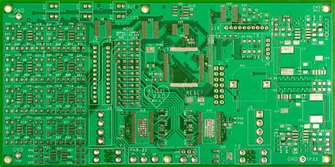
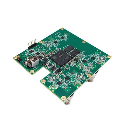
Printed Circuit Board (PCB) assembly is a critical process in the electronics manufacturing industry. It involves the placement and soldering of electronic components onto a PCB to create a functional electronic device. The PCB serves as the backbone of most electronic devices, providing mechanical support and electrical connections between components. This article delves into the various aspects of PCB assembly, including the types of PCBs, the assembly process, key technologies, challenges, and future trends.
Types of PCBs
PCBs come in various types, each suited for specific applications. The most common types include:
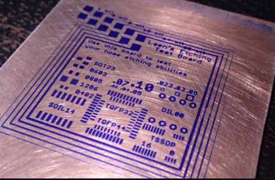
- Single-Sided PCBs: These have conductive material on one side only. They are simple and cost-effective, suitable for basic electronic devices.
- Double-sided PCBs: These have conductive material on both sides, allowing for more complex circuits. They are used in more advanced electronic devices.
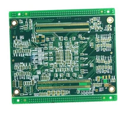
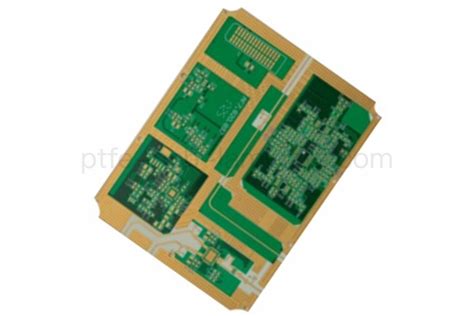
- Multi-layer PCBs: These consist of multiple layers of conductive material separated by insulating layers. They are used in high-density and high-performance applications, such as smartphones and computers.
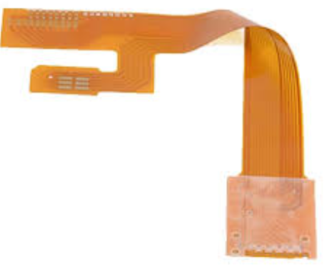
- Flexible PCBs: These are made from flexible materials, allowing them to bend and fold. They are used in applications where space and weight are critical, such as wearable devices.
- Rigid-Flex PCBs: These combine rigid and flexible PCBs, offering the benefits of both. They are used in complex applications like aerospace and medical devices.
The PCB Assembly Process
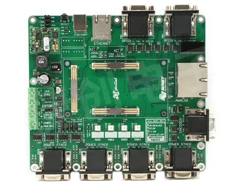
The PCB assembly process involves several steps, each crucial to ensuring the final product’s functionality and reliability. The main steps include:
- Design and Layout: The process begins with the design of the PCB using specialized software. The layout includes the placement of components and the routing of electrical connections.
- Stencil Creation: A stencil is created to apply solder paste to the PCB. The stencil ensures precise application of solder paste to the pads where components will be placed.
- Solder Paste Application: Solder paste, a mixture of tiny solder particles and flux, is applied to the PCB using the stencil. The paste holds the components in place and forms the electrical connections during soldering.
- Component Placement: Components are placed onto the PCB using automated machines called pick-and-place machines. These machines can place thousands of components per hour with high precision.
- Reflow Soldering: The PCB is passed through a reflow oven, where the solder paste is heated to melt the solder particles, forming permanent electrical connections between the components and the PCB.
- Inspection and Testing: After soldering, the PCB undergoes inspection and testing to ensure all components are correctly placed and soldered. Automated Optical Inspection (AOI) and X-ray inspection are commonly used.
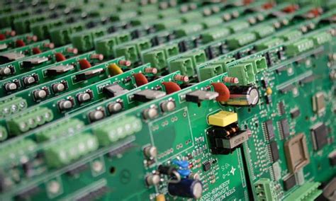
- Through-Hole Component Insertion: For components that cannot be surface-mounted, through-hole technology is used. Components are inserted into holes in the PCB and soldered on the opposite side.
- Wave Soldering: For through-hole components, wave soldering is used. The PCB is passed over a wave of molten solder, which solders the components to the board.
- Cleaning: The PCB is cleaned to remove any flux residues or contaminants that could affect performance.
- Final Inspection and Testing: The assembled PCB undergoes final inspection and functional testing to ensure it meets the required specifications.
Key Technologies in PCB Assembly
Several technologies play a crucial role in the PCB assembly process:
- Surface Mount Technology (SMT): SMT is the most widely used technology in PCB assembly. It involves placing components directly onto the surface of the PCB. SMT allows for smaller components and higher circuit density.
- Through-Hole Technology (THT): THT involves inserting component leads into holes drilled in the PCB and soldering them on the opposite side. THT is used for larger components or those requiring stronger mechanical bonds.
- Automated Optical Inspection (AOI): AOI uses cameras and software to inspect the PCB for defects such as missing components, misaligned components, and solder bridges.
- X-ray Inspection: X-ray inspection is used to inspect hidden solder joints, such as those under Ball Grid Array (BGA) components.
- Reflow Soldering: Reflow soldering is the process of melting solder paste to form electrical connections. It is a critical step in SMT assembly.
- Wave Soldering: Wave soldering is used for THT components. The PCB is passed over a wave of molten solder, which solders the components to the board.
- Selective Soldering: Selective soldering is used for soldering specific areas of the PCB, avoiding areas that cannot withstand high temperatures.
Challenges in PCB Assembly
PCB assembly is a complex process that presents several challenges:
- Miniaturization: As electronic devices become smaller, PCBs must accommodate smaller components and higher circuit density. This requires advanced manufacturing techniques and precision.
- Component Availability: The global supply chain for electronic components can be unpredictable, leading to shortages and delays.
- Thermal Management: High-density PCBs generate more heat, requiring effective thermal management to prevent overheating and ensure reliability.
- Quality Control: Ensuring the quality of the assembled PCB is critical. Defects can lead to device failure and costly recalls.
- Environmental Regulations: PCB assembly must comply with environmental regulations, such as the Restriction of Hazardous Substances (RoHS) directive, which restricts the use of certain hazardous materials.
Future Trends in PCB Assembly
The PCB assembly industry is continuously evolving, driven by advancements in technology and changing market demands. Some of the key trends shaping the future of PCB assembly include:
- Increased Automation: Automation is becoming more prevalent in PCB assembly, with advanced robotics and AI-driven systems improving efficiency and precision.
- 3D Printing: 3D printing is being explored for PCB manufacturing, allowing for rapid prototyping and customization.
- Flexible and Stretchable PCBs: The demand for flexible and stretchable PCBs is growing, driven by applications in wearable devices and IoT.
- Advanced Materials: New materials with improved thermal and electrical properties are being developed, enabling higher performance and reliability.
- Sustainability: There is a growing focus on sustainability in PCB assembly, with efforts to reduce waste, use eco-friendly materials, and improve energy efficiency.
- Integration with IoT: The integration of PCBs with IoT devices is driving the development of smart, connected PCBs with embedded sensors and communication capabilities.
- High-Speed PCBs: The demand for high-speed PCBs is increasing, driven by applications in 5G, AI, and high-performance computing.
Conclusion
PCB assembly is a vital process in the electronics manufacturing industry, enabling the creation of complex and high-performance electronic devices. The process involves several steps, from design and component placement to soldering and testing. Key technologies such as SMT, THT, AOI, and reflow soldering play a crucial role in ensuring the quality and reliability of the assembled PCB. Despite the challenges, the industry is evolving with advancements in automation, materials, and sustainability. As technology continues to advance, PCB assembly will remain at the forefront of innovation, driving the development of next-generation electronic devices.

