Printed Circuit Board (PCB) Debugging Steps: A Comprehensive Guide
Introduction
Printed Circuit Boards (PCBs) are the backbone of modern electronics, found in everything from consumer gadgets to industrial machinery. However, even a well-designed PCB can encounter issues during prototyping or production. Debugging is a critical process to identify and resolve these problems, ensuring the board functions as intended.
This guide outlines a systematic approach to PCB debugging, covering visual inspection, power checks, signal verification, and functional testing. Following these steps can save time, reduce costs, and improve reliability in PCB development.
1. Visual Inspection
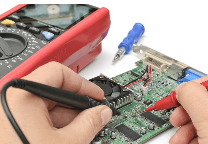
Before applying power, conduct a thorough visual inspection to identify obvious defects:
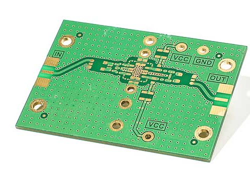
A. Component Placement & Soldering
- Verify that all components are correctly placed according to the schematic.
- Check for cold solder joints, bridges, or missing connections.
- Inspect polarized components (e.g., capacitors, diodes) for correct orientation.
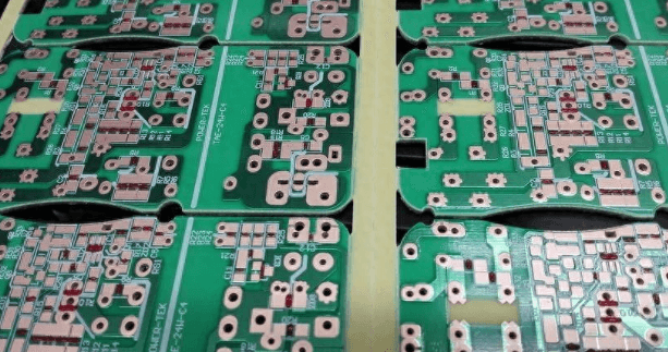
B. PCB Traces & Shorts
- Examine traces for breaks, hairline cracks, or manufacturing defects.
- Use a magnifying glass or microscope to detect tiny solder splashes causing shorts.
- Ensure no unintended connections between adjacent traces.
C. Mechanical Integrity
- Check for damaged connectors, bent pins, or loose mounting holes.
- Verify that mechanical components (switches, buttons) are properly seated.
Tools Used:
- Magnifying glass / Microscope
- Multimeter (continuity mode)
2. Power Supply Verification
A faulty power supply can lead to erratic behavior or component damage. Follow these steps:
A. Check Voltage Levels
- Measure input voltage at the power connector.
- Verify regulator outputs (e.g., 3.3V, 5V, 12V) match expected values.
- Look for voltage drops under load (indicating poor power delivery).
B. Test for Shorts
- Use a multimeter in resistance mode to check for shorts between power and ground.
- If a short is detected, isolate sections of the PCB (e.g., remove ICs) to locate the fault.
C. Monitor Current Draw
- Use a current-limited power supply to avoid damaging components.
- Excessive current may indicate a short or defective component.
Tools Used:
- Multimeter (voltage, resistance modes)
- Bench power supply (with current limiting)
- Oscilloscope (for ripple/noise analysis)
3. Signal Integrity & Functional Testing
After confirming power stability, proceed to test signal paths and functionality.
A. Clock & Reset Signals
- Verify clock signals (e.g., crystal oscillators) with an oscilloscope.
- Ensure reset circuits function correctly (e.g., voltage levels, timing).
B. Digital Communication Lines (I2C, SPI, UART)
- Use a logic analyzer or oscilloscope to check signal integrity.
- Look for noise, ringing, or incorrect voltage levels.
- Verify data transmission between microcontrollers and peripherals.
C. Analog Circuit Testing
- Check amplifier outputs, sensor readings, and filter responses.
- Compare measured values against expected behavior.
Tools Used:
- Oscilloscope
- Logic analyzer
- Signal generator (for analog stimulus)

4. Firmware & Software Debugging
If the PCB includes a microcontroller or FPGA, firmware issues may cause malfunctions.
A. Verify Program Execution
- Check if the MCU boots (e.g., LED blink test).
- Use debugging tools (JTAG, SWD) to step through code.
B. Check Peripheral Initialization
- Ensure GPIO, ADC, PWM, and communication interfaces are configured correctly.
- Review datasheets for register settings.
C. Log Debug Data
- Use UART or SWO (Serial Wire Output) for real-time debugging.
- Monitor variables and system states.
Tools Used:
- Debugger (ST-Link, J-Link, etc.)
- Serial terminal (PuTTY, Tera Term)
5. Thermal & Environmental Testing
Some issues appear only under specific conditions.
A. Thermal Analysis
- Run the PCB under load and monitor component temperatures.
- Use a thermal camera to detect hotspots.
B. Vibration & Environmental Stress
- Test in different environments (temperature, humidity).
- Check for loose connections under mechanical stress.
Tools Used:
- Thermal camera
- Environmental chamber (if available)
6. Final Validation & Documentation
After resolving issues, perform a full system test:
- Validate all functions against design specifications.
- Document fixes for future reference.
Conclusion
PCB debugging requires a methodical approach, combining visual inspection, electrical testing, and firmware validation. By following these steps, engineers can efficiently identify and resolve issues, ensuring reliable PCB performance.