Printed Circuit Board PCBA: Key Advances Shaping Electronics

Key Takeaways
The evolution of PCB assembly (PCBA) technologies is driving transformative shifts across electronics manufacturing. Innovations such as high-density interconnect (HDI) designs enable compact, high-performance devices, while breakthroughs in flexible substrates empower wearables and foldable electronics. The integration of IoT-ready PCBA solutions ensures seamless connectivity, with embedded sensors and real-time data analytics optimizing device functionality.
| Aspect | Traditional Approach | Advanced Innovation | Impact |
|---|---|---|---|
| HDI Designs | Limited layer counts | Microvias & stacked interconnects | 50% smaller footprints |
| Flexible PCBA | Rigid FR-4 materials | Polyimide-based substrates | Bend radii under 1mm |
| 5G Optimization | Standard RF layouts | Millimeter-wave antenna integration | 10x faster signal transmission |
Meanwhile, 5G-ready PCBA manufacturing addresses high-frequency signal integrity through advanced materials like low-loss laminates. Sustainability gains momentum with lead-free soldering and recyclable substrates, reducing e-waste by up to 30%. However, challenges persist in thermal management for high-density PCB assembly, solved via liquid cooling and thermally conductive adhesives. As smart factories adopt AI-driven inspection systems, defect rates drop below 0.1%, ensuring scalable production of next-gen electronics.
HDI PCB Innovations Reshape Electronics
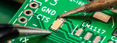
The relentless push for miniaturization and enhanced performance in modern electronics has driven groundbreaking advancements in High-Density Interconnect (HDI) PCB technology. By leveraging laser-drilled microvias, stacked copper layers, and ultra-fine trace geometries, HDI designs enable PCB assembly (PCBA) processes to integrate more components into smaller footprints while maintaining signal integrity. This is particularly critical for applications like 5G infrastructure and wearable devices, where power efficiency and thermal management are non-negotiable.
Design Tip: When implementing HDI layouts, prioritize material selection to balance thermal expansion coefficients and high-frequency signal performance.
A key innovation lies in sequential lamination techniques, which allow manufacturers to build multilayer boards with precision. These methods reduce parasitic capacitance and crosstalk, addressing challenges in high-density PCB assembly. Additionally, the adoption of embedded passive components within HDI structures streamlines PCBA workflows, cutting production time by up to 30%. However, achieving defect-free soldering on densely packed boards demands advanced inspection systems, such as automated optical alignment paired with X-ray tomography.
As IoT and AI-driven devices demand faster data processing, HDI’s role in enabling shorter signal paths and lower latency becomes indispensable. This evolution underscores the need for collaboration between PCB designers and PCBA specialists to optimize manufacturability without compromising performance.
Flexible PCBA Substrate Breakthroughs
Recent advances in flexible PCBA substrates are redefining design possibilities for modern electronics. Unlike traditional rigid boards, polyimide-based materials and liquid crystal polymer (LCP) films now enable ultra-thin, bendable circuits that maintain performance under repeated stress. These breakthroughs address growing demands for PCB assembly in wearables, medical implants, and foldable devices, where space constraints and dynamic movement are critical.
A key innovation lies in hybrid architectures combining flexible PCBA layers with rigid sections, optimizing both durability and component density. Manufacturers now utilize laser-direct structuring (LDS) and additive printing techniques to embed circuitry on curved surfaces, reducing interconnect failures by up to 40%. Additionally, thermally stable substrates withstand temperatures exceeding 200°C, supporting high-power applications like automotive sensors.
The shift toward 3D-printed circuitry further accelerates prototyping cycles, allowing rapid iteration for IoT and 5G-enabled devices. Notably, these substrates integrate seamlessly with PCB assembly processes, minimizing retooling costs while enhancing signal integrity in high-frequency environments. As industries prioritize lightweight, eco-friendly designs, recyclable flexible materials are emerging—cutting e-waste without compromising electrical performance. This progress not only expands application horizons but also reinforces the role of PCBA innovation in driving next-generation electronics.
IoT-Driven PCB Assembly Innovations
The integration of IoT (Internet of Things) into PCB assembly processes is revolutionizing how devices communicate, operate, and adapt in real time. Modern PCBA designs now prioritize miniaturized components and low-power architectures to support energy-efficient sensors and wireless modules critical for IoT ecosystems. Advanced surface-mount technology (SMT) enables tighter component placement, ensuring seamless connectivity for smart devices—from wearables to industrial monitors.
A key innovation lies in embedded systems, where microcontrollers and RF transceivers are directly integrated into PCBA layouts, reducing latency and enhancing data transmission reliability. Manufacturers are also adopting automated optical inspection (AOI) systems to detect defects in high-density IoT boards, minimizing failures in mission-critical applications. Additionally, the rise of edge computing demands PCB assemblies capable of processing data locally, reducing cloud dependency while maintaining robust thermal management.
To align with sustainability goals, IoT-driven PCBA processes increasingly utilize lead-free solders and recyclable substrates, balancing performance with environmental responsibility. These advancements not only optimize device functionality but also pave the way for scalable, interconnected networks—a foundation for the next phase of 5G-ready electronics discussed in subsequent sections.
5G-Ready PCBA Manufacturing Techniques
The transition to 5G networks demands unprecedented precision in PCB assembly, driving innovations in PCBA manufacturing processes. High-frequency signal integrity now governs material selection, with manufacturers adopting low-loss laminates like PTFE-based substrates to minimize dielectric losses above 6 GHz. Advanced laser direct imaging (LDI) systems enable micron-level trace accuracy, critical for maintaining impedance control in 5G-ready PCBA designs. To address heat dissipation challenges from increased component density, hybrid cooling solutions—such as embedded thermal vias and ceramic-filled solder masks—are becoming standard.
Automated automated optical inspection (AOI) systems, enhanced with AI-driven defect detection, now validate high-density interconnects (HDIs) at speeds matching 5G production volumes. Meanwhile, modular assembly lines integrate mmWave testing protocols directly into PCBA workflows, ensuring compliance with 3GPP Release 16 standards. This shift also prioritizes sustainability, with lead-free solders and halogen-free substrates reducing environmental impact without compromising signal performance. By aligning PCB assembly techniques with 5G’s technical demands, manufacturers are enabling faster data rates, ultra-low latency, and reliable connectivity for next-gen IoT and edge computing devices.
Sustainable Electronics Via PCBA Evolution
The drive toward sustainable electronics is fundamentally reshaping PCB assembly methodologies, with PCBA innovations leading the charge. Manufacturers now prioritize lead-free soldering and halogen-free substrates, reducing hazardous waste while maintaining performance standards. Advanced PCBA techniques, such as laser-based depaneling and precision solder paste application, minimize material waste by optimizing component placement accuracy.
A critical shift involves integrating recyclable polymers and biodegradable laminates into PCB assembly workflows, enabling easier disassembly and material recovery at end-of-life stages. Energy-efficient manufacturing processes, including low-temperature soldering and solar-powered production lines, further cut carbon footprints. The adoption of IoT-enabled monitoring systems in PCBA lines enhances resource management, dynamically adjusting energy use and reducing excess consumption.
These advancements align with circular economy principles, where modular PCBA designs allow selective upgrades rather than full-board replacements. For instance, 5G-ready assemblies now incorporate standardized connectors and replaceable RF modules, extending product lifespans. As regulatory pressures mount, the industry’s focus on green chemistry and closed-loop recycling systems positions PCBA as a cornerstone of eco-conscious electronics manufacturing.
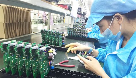
Smart Factories Transform PCB Production
The integration of IoT-driven automation and AI-powered analytics is revolutionizing PCB assembly workflows, enabling real-time monitoring and adaptive manufacturing systems. Smart factories leverage industrial IoT sensors to track every stage of PCBA production, from component placement to soldering precision, ensuring minimal deviations in high-volume batches. Advanced machine learning algorithms analyze historical data to predict equipment maintenance needs, reducing downtime by up to 30% while optimizing throughput.
Modular production lines now dynamically adjust to design changes, allowing seamless transitions between high-density interconnect (HDI) layouts and flexible PCB configurations without manual recalibration. This agility is critical for meeting 5G and IoT device demands, where rapid prototyping and scalability are paramount. Additionally, digital twin technology simulates PCBA processes virtually, identifying potential defects before physical production begins—a key step toward zero-waste manufacturing.
As these systems evolve, they address longstanding challenges in PCB assembly, such as thermal management in compact designs, while aligning with global sustainability goals through energy-efficient practices. The shift to smart factories not only accelerates time-to-market but also strengthens supply chain resilience, positioning PCBA at the core of next-generation electronics ecosystems.
High-Density PCB Assembly Challenges Solved
Advancements in PCB assembly techniques are overcoming longstanding barriers in high-density interconnect (HDI) designs, enabling smaller yet more powerful electronic devices. As components shrink and functionality expands, traditional PCBA methods struggle with signal integrity and thermal management. Modern solutions now integrate laser-drilled microvias and sequential lamination processes, reducing crosstalk while maintaining structural stability. Automated optical inspection (AOI) systems paired with machine learning algorithms detect micron-level defects, ensuring reliability in densely packed layouts.
Material innovations also play a critical role. High-performance substrates like polyimide-flex hybrids withstand repeated thermal cycling, addressing warping risks in multilayer stacks. Additionally, embedded component technology eliminates surface-mounted parts, freeing up space for critical traces. For power-hungry applications, advanced thermal vias and copper-filled trenches dissipate heat efficiently, preventing performance throttling.
These breakthroughs align with demands for 5G-ready PCBA and IoT devices, where miniaturization cannot compromise speed or durability. By combining precision robotics with AI-driven design software, manufacturers now achieve sub-6μm trace widths without sacrificing yield rates—a feat once deemed unattainable. This progress not only resolves HDI challenges but sets new benchmarks for next-generation electronics.
Conclusion
The evolution of PCB assembly technologies underscores a transformative era in electronics manufacturing. From HDI designs enabling ultra-compact devices to flexible substrates powering wearable tech, PCBA advancements are redefining performance benchmarks. Innovations like IoT-integrated assemblies and 5G-ready manufacturing techniques highlight the industry’s shift toward interconnected, high-speed systems, while sustainable practices—such as lead-free soldering and recyclable materials—address growing environmental demands.
Smart factories, leveraging AI-driven quality control and automated PCB assembly lines, exemplify how digitalization boosts precision and scalability. These developments not only resolve challenges in high-density interconnects but also pave the way for next-gen applications in automotive, healthcare, and aerospace. As PCBA processes continue to prioritize energy efficiency and miniaturization, the synergy between cutting-edge engineering and eco-conscious production will remain pivotal. Moving forward, the convergence of these innovations ensures electronics manufacturing stays agile, meeting both current needs and future technological horizons.
FAQs
How does HDI technology improve modern PCB assembly processes?
High-Density Interconnect (HDI) designs enable tighter component placement and finer traces, reducing signal loss in PCBA for 5G and IoT devices. This advancement supports faster data transmission while minimizing board size.
What makes flexible substrates critical for next-gen electronics?
Flexible substrates allow PCB assembly on bendable materials, ideal for wearables and medical devices. Innovations in polyimide-based PCBA enhance durability and thermal stability, enabling compact, lightweight solutions.
How is IoT integration reshaping PCB assembly workflows?
IoT demands embedded sensors and wireless modules in PCBA, requiring precise soldering and multi-layer stacking. Automated optical inspection (AOI) ensures reliability in high-mix, low-volume production for smart devices.
Why are 5G-ready assemblies more complex than traditional designs?
5G PCBA requires ultra-low latency and high-frequency signal integrity. Techniques like laser-drilled microvias and advanced EMI shielding mitigate interference, ensuring consistent performance in mmWave applications.
Can sustainable practices coexist with high-performance PCB assembly?
Yes. Lead-free soldering, recyclable substrates, and energy-efficient manufacturing reduce the environmental footprint of PCBA without compromising quality. Companies now prioritize RoHS compliance and closed-loop material recovery.
What challenges arise in high-density PCB assembly for smart factories?
Microcomponent placement (e.g., 0201 packages) demands precision pick-and-place systems. Real-time monitoring via AI-driven analytics optimizes yield rates, addressing alignment and soldering defects in complex PCBA layouts.
Ready to Elevate Your PCB Assembly Project?
For expert guidance on optimizing your next PCBA design, please click here to explore tailored solutions for IoT, 5G, and high-density applications.