Printed wiring boards
Evolution Of Printed Wiring Boards: From Inception To Modern Applications
The evolution of printed wiring boards (PWBs) is a fascinating journey that reflects the broader advancements in technology and manufacturing processes over the past century. Initially conceived in the early 20th century, printed wiring boards have undergone significant transformations, adapting to the ever-increasing demands of modern electronics. This evolution is not only a testament to human ingenuity but also a reflection of the relentless pursuit of efficiency and miniaturization in electronic devices.
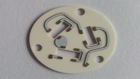
The inception of printed wiring boards can be traced back to the 1900s when the need for a more efficient method of connecting electronic components became apparent. Before PWBs, point-to-point wiring was the norm, a labor-intensive and error-prone process that limited the complexity and reliability of electronic devices. The introduction of PWBs revolutionized this process by providing a standardized platform for mounting and interconnecting components. The early versions of PWBs were simple, single-sided boards with copper tracks etched onto a non-conductive substrate. This innovation significantly reduced the size and weight of electronic devices, paving the way for more compact and reliable products.
As technology advanced, so did the complexity of printed wiring boards.
The development of double-sided and multilayer boards in the mid-20th century marked a significant milestone in the evolution of PWBs. These advancements allowed for more intricate circuit designs, enabling the integration of a greater number of components on a single board. The introduction of through-hole technology further enhanced the reliability and performance of PWBs by providing robust mechanical and electrical connections between layers. This period also saw the rise of automated manufacturing processes, which improved the precision and consistency of PWB production.
Transitioning into the late 20th and early 21st centuries, the demand for smaller, faster, and more powerful electronic devices drove further innovations in PWB technology.
The advent of surface mount technology (SMT) revolutionized the industry by allowing components to be mounted directly onto the surface of the board, eliminating the need for through-hole connections. This development not only reduced the size and weight of electronic assemblies but also increased their performance and reliability. Additionally, the use of advanced materials and fabrication techniques, such as flexible and rigid-flex boards, expanded the range of applications for PWBs, enabling their use in a variety of industries, from consumer electronics to aerospace and medical devices.
In recent years, the evolution of printed wiring boards has been characterized by the integration of cutting-edge technologies and materials.
The rise of high-density interconnect (HDI) boards, which feature finer lines and spaces, smaller vias, and higher connection pad density, has enabled the development of increasingly compact and complex electronic devices. Furthermore, the incorporation of advanced materials, such as high-frequency laminates and thermal management solutions, has enhanced the performance and reliability of PWBs in demanding applications.
Looking ahead, the future of printed wiring boards is poised to be shaped by emerging technologies and trends.
The growing interest in the Internet of Things (IoT), wearable technology, and 5G communications is expected to drive further innovations in PWB design and manufacturing. Additionally, the increasing focus on sustainability and environmental responsibility is likely to influence the development of eco-friendly materials and processes in the PWB industry. As printed wiring boards continue to evolve, they will undoubtedly play a crucial role in the advancement of electronic technology, enabling the creation of more sophisticated and efficient devices that will shape the world of tomorrow.
Key Materials And Technologies In Printed Wiring Board Manufacturing
Printed wiring boards (PWBs), commonly known as printed circuit boards (PCBs), are the backbone of modern electronic devices, providing the necessary mechanical support and electrical connections for various components. The manufacturing of PWBs involves a complex interplay of materials and technologies, each contributing to the board’s functionality, reliability, and performance. Understanding these key materials and technologies is essential for anyone involved in the electronics industry.
To begin with, the substrate material forms the foundation of any PWB.
Typically, the most common substrate used is FR-4, a composite material made of woven fiberglass cloth with an epoxy resin binder that is flame resistant. FR-4 is favored for its excellent mechanical strength, thermal resistance, and electrical insulation properties. However, for applications requiring higher performance, such as in aerospace or high-frequency communications, alternative materials like polyimide, PTFE (Teflon), or ceramic substrates may be employed. These materials offer superior thermal stability and dielectric properties, albeit at a higher cost.
Transitioning from substrates to conductive materials, copper is the predominant choice for creating the conductive pathways on a PWB.
Copper’s excellent electrical conductivity and relatively low cost make it ideal for this purpose. The copper is typically laminated onto the substrate and then etched away to form the desired circuit patterns. This etching process is a critical step in PWB manufacturing, requiring precision to ensure that the pathways are accurately formed without defects.
In addition to the substrate and conductive materials, the solder mask is another crucial component in PWB manufacturing.
The solder mask is a protective layer applied over the copper traces to prevent oxidation and to insulate the board against short circuits. It also helps in the soldering process by keeping the solder confined to the designated pads. The solder mask is usually green, although other colors are available, and is made from a polymer-based material that can withstand the high temperatures of soldering.
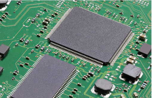
Moving on to the technologies involved, one of the most significant advancements in PWB manufacturing is the development of surface mount technology (SMT).
SMT allows for the placement of components directly onto the surface of the board, as opposed to the older through-hole technology, which required components to be inserted into drilled holes. SMT offers numerous advantages, including reduced board size, increased component density, and improved performance due to shorter electrical paths. This technology has become the standard in modern electronics manufacturing.
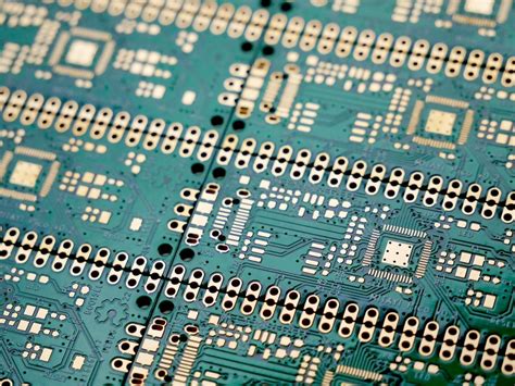
Furthermore, the advent of multilayer PWBs has revolutionized the industry by allowing for more complex and compact designs. Multilayer boards consist of multiple layers of substrate and circuitry stacked together, interconnected by vias. This design enables more intricate circuit patterns and greater functionality within a smaller footprint, which is essential for today’s compact electronic devices.
In conclusion, the manufacturing of printed wiring boards is a sophisticated process that relies on a combination of advanced materials and technologies. From the choice of substrate and conductive materials to the application of solder masks and the implementation of surface mount technology, each element plays a vital role in the final product’s performance. As technology continues to evolve, so too will the materials and methods used in PWB manufacturing, driving further innovation in the electronics industry.
Environmental Impact And Sustainability In Printed Wiring Board Production
Printed wiring boards (PWBs), commonly known as printed circuit boards (PCBs), are integral components in modern electronic devices, serving as the backbone for electrical connectivity and functionality. As the demand for electronic devices continues to surge, the environmental impact and sustainability of PWB production have become increasingly significant concerns. The production process of PWBs involves several stages, each with its own environmental implications, from raw material extraction to manufacturing and disposal.
To begin with, the raw materials used in PWB production, such as copper, fiberglass, and various chemicals, have notable environmental footprints.
Copper mining, for instance, is energy-intensive and often results in habitat destruction and soil and water pollution. The extraction and processing of these materials contribute to greenhouse gas emissions, which exacerbate climate change. Furthermore, the use of hazardous chemicals in the etching and plating processes poses risks to both human health and the environment. These chemicals, if not managed properly, can lead to contamination of water sources and soil, affecting ecosystems and communities.
In response to these challenges, the industry has been exploring more sustainable practices.
One approach is the adoption of cleaner production techniques that minimize waste and reduce the use of toxic substances. For example, some manufacturers are implementing closed-loop systems that recycle water and chemicals, thereby reducing the release of pollutants. Additionally, advancements in technology have led to the development of alternative materials that are less harmful to the environment. For instance, some companies are experimenting with biodegradable substrates and lead-free soldering materials, which can significantly reduce the environmental impact of PWBs.
Moreover, the concept of design for the environment (DfE) is gaining traction in the PWB industry.
This approach involves designing products with their entire lifecycle in mind, from production to disposal. By considering factors such as material selection, energy efficiency, and end-of-life management during the design phase, manufacturers can create PWBs that are easier to recycle and have a lower environmental impact. For example, modular designs that allow for easy disassembly can facilitate the recycling process, ensuring that valuable materials are recovered and reused rather than ending up in landfills.
In addition to production and design improvements, the industry is also focusing on enhancing the recyclability of PWBs.
Recycling not only conserves resources but also reduces the need for raw material extraction, thereby mitigating some of the environmental impacts associated with mining and processing. However, recycling PWBs is a complex process due to the diverse materials and components involved. To address this, researchers are developing more efficient recycling technologies that can recover a higher percentage of materials from discarded PWBs.
While significant progress has been made, challenges remain in achieving full sustainability in PWB production.
Regulatory frameworks and industry standards play a crucial role in driving environmental improvements. Governments and industry bodies are increasingly setting stricter regulations and guidelines to ensure that manufacturers adhere to sustainable practices. Collaboration among stakeholders, including manufacturers, suppliers, and policymakers, is essential to advancing sustainability in the PWB industry.
In conclusion, the environmental impact and sustainability of printed wiring board production are critical issues that require concerted efforts from all stakeholders. By adopting cleaner production techniques, embracing design for the environment principles, and improving recycling processes, the industry can significantly reduce its environmental footprint. As technology continues to evolve, ongoing innovation and collaboration will be key to achieving a more sustainable future for PWB production.
Innovations In Printed Wiring Board Design For Enhanced Performance
Printed wiring boards (PWBs), often referred to as printed circuit boards (PCBs), are the backbone of modern electronic devices, providing the necessary mechanical support and electrical connections for various components. As technology continues to advance, the demand for more efficient, reliable, and compact electronic devices has driven significant innovations in PWB design. These innovations aim to enhance performance, reduce costs, and meet the ever-evolving needs of industries ranging from consumer electronics to aerospace.
One of the most notable advancements in PWB design is the development of high-density interconnect (HDI) technology.
HDI boards are characterized by their finer lines and spaces, smaller vias, and higher connection pad density. This technology allows for more components to be placed on a single board, thereby reducing the overall size and weight of electronic devices. The miniaturization of components and the increased functionality of devices are made possible through HDI, which is particularly beneficial in the production of smartphones, tablets, and other portable electronics.
In addition to HDI, the integration of flexible and rigid-flex PWBs has revolutionized the design and functionality of electronic devices.
Flexible PWBs are made from materials that allow them to bend and flex, making them ideal for applications where space is limited or where the board must conform to a specific shape. Rigid-flex boards combine the benefits of both rigid and flexible PWBs, offering enhanced durability and reliability. These boards are increasingly used in medical devices, military equipment, and consumer electronics, where their ability to withstand harsh environments and mechanical stress is crucial.
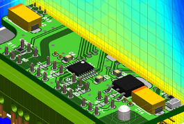
Another significant innovation in PWB design is the use of advanced materials that improve thermal management and electrical performance.
As electronic devices become more powerful, they generate more heat, which can affect performance and reliability. To address this issue, designers are incorporating materials with superior thermal conductivity, such as metal-core substrates and ceramic-filled polymers. These materials help dissipate heat more effectively, ensuring that devices operate within safe temperature ranges and maintain optimal performance.
Moreover, the adoption of additive manufacturing techniques, such as 3D printing, is transforming the way PWBs are designed and produced.
Additive manufacturing allows for greater design flexibility, enabling the creation of complex geometries that were previously difficult or impossible to achieve with traditional manufacturing methods. This technology also reduces material waste and production time, leading to cost savings and more sustainable manufacturing processes.
Furthermore, the integration of Internet of Things (IoT) technology into PWB design is opening new avenues for innovation.
IoT devices require PWBs that can support wireless communication, data processing, and energy efficiency. Designers are now focusing on creating boards that can accommodate these requirements, incorporating features such as embedded antennas and energy-harvesting components. This integration is essential for the development of smart devices that can communicate and interact with each other seamlessly.
In conclusion, the innovations in printed wiring board design are pivotal in meeting the growing demands for enhanced performance in electronic devices. Through advancements in HDI technology, flexible and rigid-flex boards, advanced materials, additive manufacturing, and IoT integration, PWBs are becoming more efficient, reliable, and versatile. As technology continues to evolve, these innovations will play a crucial role in shaping the future of electronics, enabling the development of devices that are not only more powerful but also more compact and sustainable.