Prototype PCB Manufacturing: A Comprehensive Guide
Introduction
In the world of electronics, Printed Circuit Boards (PCBs) serve as the backbone of virtually every electronic device. From smartphones to industrial machinery, PCBs are essential for connecting various components and ensuring the functionality of the device. As technology advances and the demand for faster product development increases, prototype PCB manufacturing has become a critical aspect of the electronics industry. This article delves into the process of prototype PCB manufacturing, its importance, techniques, challenges, and future trends.
What is Prototype PCB Manufacturing?
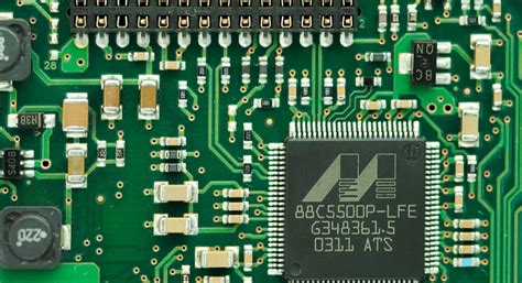
Prototype PCB manufacturing refers to the process of creating initial versions of PCBs for testing and development purposes. These prototypes allow engineers and designers to evaluate the design, functionality, and performance of the PCB before mass production. Prototyping is crucial in identifying design flaws, verifying electrical performance, and ensuring manufacturability.
Importance of Prototype PCBs
- Design Validation: Prototypes allow designers to test and validate their concepts, ensuring that the PCB meets the required specifications and functionalities.
- Cost Efficiency: By identifying issues early in the design process, companies can save significant costs associated with rework and redesign during mass production.
- Time-to-Market: Rapid prototyping enables faster iterations, allowing companies to bring their products to market more quickly.
- Risk Mitigation: Prototyping helps in identifying potential risks and challenges in the design, reducing the likelihood of failures in the final product.
The Prototype PCB Manufacturing Process
The process of prototype PCB manufacturing can be broken down into several key steps:
1. Design and Layout
The first step in PCB prototyping is the design and layout of the PCB. Engineers use Computer-Aided Design (CAD) software to create the schematic and layout. This involves:
- Schematic Design: Creating a visual representation of the circuit, including components and their connections.
- PCB Layout: Translating the schematic into a physical layout, determining the placement of components, traces, and vias.
2. Design Rule Check (DRC)
Once the design is complete, a Design Rule Check (DRC) is performed to ensure that the layout adheres to manufacturing standards. This step helps identify potential issues such as:
- Trace width violations
- Clearance violations between traces and pads
- Incorrect component placements
3. Fabrication
After the design is validated, the PCB goes into fabrication. This process involves several steps:
- Material Selection: Choosing the appropriate substrate material (e.g., FR-4, Rogers) based on the application requirements.
- Copper Layer Application: Applying a layer of copper onto the substrate, which will form the conductive pathways.
- Etching: Removing excess copper to create the desired circuit pattern.
- Drilling: Creating holes for vias and component leads.
- Plating: Adding a layer of metal to the drilled holes to create electrical connections between layers.
- Solder Mask Application: Applying a protective layer to prevent solder from bridging between traces.
- Silkscreen Printing: Adding labels and markings for components.
4. Assembly
Once the PCB is fabricated, the next step is assembly, which involves placing and soldering components onto the board. This can be done through:
- Through-Hole Technology (THT): Inserting component leads through holes and soldering them on the opposite side.
- Surface Mount Technology (SMT): Placing components directly onto the surface of the PCB and soldering them.
5. Testing
After assembly, the prototype PCB undergoes rigorous testing to ensure functionality. This may include:
- Electrical Testing: Verifying that all connections are correct and that the circuit functions as intended.
- Functional Testing: Testing the PCB within the context of the entire system to ensure it meets performance specifications.
- Environmental Testing: Assessing the PCB’s performance under various environmental conditions (temperature, humidity, etc.).
6. Iteration
Based on the testing results, engineers may need to iterate on the design. This can involve making modifications to the layout, changing component specifications, or adjusting the manufacturing process. The iterative nature of prototyping helps refine the design until it meets all requirements.
Techniques in Prototype PCB Manufacturing
Several techniques are employed in prototype PCB manufacturing, each with its advantages and considerations:
1. Rapid Prototyping
Rapid prototyping techniques, such as additive manufacturing (3D printing), allow for quick iterations of PCB designs. These methods enable designers to create physical prototypes in a fraction of the time compared to traditional methods.
2. Low-Volume Production
For prototypes that require more than just a few units, low-volume production techniques can be employed. This approach allows for small batch runs, making it cost-effective for testing and validation.
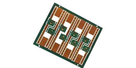
3. Flexible PCBs
Flexible PCBs are increasingly popular for prototypes, especially in applications where space is limited or where the PCB needs to conform to specific shapes. These boards can be bent and twisted without compromising functionality.
4. Hybrid PCBs
Hybrid PCBs combine different technologies, such as integrating both rigid and flexible components. This versatility allows for innovative designs that can meet complex requirements.
Challenges in Prototype PCB Manufacturing
Despite its advantages, prototype PCB manufacturing comes with its own set of challenges:
1. Design Complexity
As designs become more complex, the risk of errors increases. Ensuring that all components fit and function correctly can be a daunting task.
2. Cost Management
While prototyping can save costs in the long run, the initial investment in materials, tools, and labor can be significant. Companies must balance the need for rapid prototyping with budget constraints.
3. Time Constraints
The pressure to deliver prototypes quickly can lead to rushed designs and increased likelihood of errors. Effective project management is essential to ensure timely delivery without compromising quality.
4. Technology Limitations
Not all manufacturers have the same capabilities. Finding a manufacturer that can meet specific requirements, such as high-frequency applications or advanced materials, can be challenging.
Future Trends in Prototype PCB Manufacturing
As technology continues to evolve, several trends are shaping the future of prototype PCB manufacturing:
1. Automation and AI
The integration of automation and artificial intelligence in the design and manufacturing process is expected to streamline operations, reduce errors, and enhance efficiency.
2. Advanced Materials
The development of new materials, such as high-frequency substrates and environmentally friendly options, will expand the possibilities for PCB design and functionality.
3. Internet of Things (IoT)
With the rise of IoT devices, the demand for compact, efficient, and reliable PCBs will continue to grow. Prototyping methods will need to adapt to meet these evolving requirements.
4. Sustainability
There is a growing emphasis on sustainable practices in PCB manufacturing. Companies are increasingly seeking eco-friendly materials and processes to reduce their environmental impact.
Conclusion
Prototype PCB manufacturing is a vital process that enables engineers and designers to bring their ideas to life. By facilitating rapid testing and iteration, prototyping helps ensure that final products meet quality and performance standards. While challenges exist, advancements in technology and techniques continue to enhance the efficiency and effectiveness of PCB prototyping. As the electronics industry evolves, staying abreast of these trends will be crucial for companies looking to maintain a competitive edge.


