Prototype SMT Assembly: Accelerating Electronics Development Cycles
Key Takeaways
Modern PCB assembly processes, particularly SMT (Surface Mount Technology) prototyping, have become pivotal in accelerating electronics development. By integrating rapid prototyping with PCBA (Printed Circuit Board Assembly) workflows, engineers can validate designs faster while maintaining micron-level accuracy in component placement. This precision reduces iterative delays, enabling teams to transition seamlessly from concept to functional prototypes.
Scalable SMT solutions further enhance agility, allowing manufacturers to adjust batch sizes dynamically—whether testing a single-board design or preparing for mid-volume pre-production. Rigorous electrical and thermal testing protocols embedded within prototype SMT assembly ensure compliance with industry standards, minimizing post-deployment failures.
The synergy between automated pick-and-place systems and advanced PCB assembly software slashes time-to-market by up to 40%, a critical advantage in sectors like IoT, automotive, and medical devices. Cross-industry adoption of SMT techniques demonstrates their versatility, from optimizing signal integrity in high-frequency circuits to ensuring durability in harsh environments.
By prioritizing cost-effective prototyping strategies, companies mitigate financial risks during R&D while maintaining readiness for mass production—proving that strategic PCBA investments directly correlate with market responsiveness and product performance.
Streamlining Electronics Development via SMT
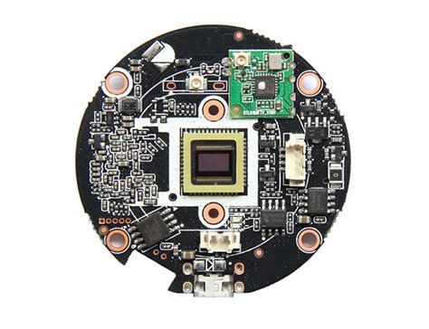
Modern electronics development relies heavily on Surface Mount Technology (SMT) to accelerate prototyping and refine product designs. By integrating PCB assembly processes with automated SMT workflows, engineers can achieve sub-millimeter precision in component placement, reducing manual errors and enabling rapid design validation. The transition from traditional through-hole methods to PCBA-optimized SMT workflows allows for compact, high-density layouts critical for IoT devices, wearables, and industrial control systems.
Tip: For teams aiming to shorten iteration cycles, partnering with SMT-focused PCB assembly providers ensures access to advanced pick-and-place systems and reflow ovens, which are essential for maintaining consistency in prototype batches.
A key advantage of SMT-driven prototyping lies in its scalability. Early-stage PCBA prototypes can seamlessly transition to mass production with minimal retooling, thanks to standardized solder paste application and component libraries. This flexibility supports agile testing of thermal management, signal integrity, and power distribution across multiple design revisions. Additionally, SMT’s compatibility with mixed-technology boards (combining surface-mount and through-hole components) simplifies functional testing for hybrid systems.
By leveraging SMT’s precision and repeatability, developers mitigate risks associated with design flaws while compressing timelines—a critical factor in industries like automotive and medical devices, where regulatory compliance and performance reliability are non-negotiable.
Precision Manufacturing in SMT Prototyping
Modern PCB assembly processes rely on precision manufacturing techniques to ensure prototype reliability. Automated pick-and-place systems achieve micron-level accuracy when positioning components on boards, minimizing placement errors that could compromise functionality. Advanced soldering methods, such as reflow or vapor phase techniques, create consistent electrical connections while managing thermal stress on sensitive parts. These processes are critical in PCBA prototyping, where even minor deviations can lead to cascading failures during testing phases.
Furthermore, precision extends to material selection, with engineers specifying high-tolerance substrates and low-voiding solder pastes to meet application-specific demands. Real-time optical inspection systems validate each assembly step, ensuring compliance with design specifications before prototypes proceed to functional validation. This meticulous approach not only accelerates debugging but also establishes a foundation for scalable production by identifying potential manufacturability issues early.
By maintaining strict process controls during SMT prototyping, teams reduce iterative redesigns and create robust prototypes that mirror final-product performance across diverse operating conditions.
Scalable Solutions for Rapid Product Iteration
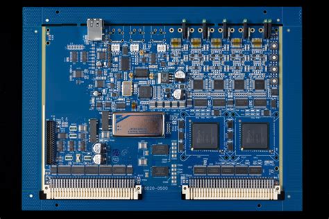
Modern PCB assembly workflows leverage scalable SMT processes to support dynamic product development demands. By integrating modular design principles with automated PCBA production lines, manufacturers can seamlessly transition from low-volume prototyping to high-volume manufacturing without compromising precision. This flexibility enables engineers to test multiple design iterations in parallel, refining functionality while maintaining alignment with market timelines. Advanced SMT assembly platforms employ adaptive tooling configurations and component placement algorithms, allowing rapid reconfiguration for diverse board geometries or material specifications.
A key advantage lies in the ability to replicate full-scale production conditions during prototyping phases. For instance, automated pick-and-place systems and precision reflow ovens used in PCBA processes ensure consistent solder joint quality across prototype batches, reducing post-production debugging cycles. Manufacturers further enhance scalability through cloud-based process monitoring, which aggregates real-time data from PCB assembly stages to optimize material utilization and throughput. These systems enable predictive adjustments to solder paste application or thermal profiles, addressing potential yield issues before mass production.
By bridging the gap between prototype validation and commercial deployment, scalable SMT assembly solutions empower innovators to accelerate iteration velocity while preserving cost-efficiency and performance validation benchmarks. This approach proves critical in industries like IoT and automotive electronics, where evolving standards demand continuous hardware refinements within compressed development windows.
Rigorous Testing in Prototype Assembly Processes
Modern PCB assembly workflows integrate multi-stage validation protocols to ensure prototype reliability before scaling. Surface-mount technology (SMT) prototypes undergo automated optical inspection (AOI) and X-ray testing to detect micro-scale defects like solder bridging or component misalignment. These tests are critical in PCBA development, as even minor flaws in high-density layouts can cascade into systemic failures during field deployment.
| Test Type | Method | Purpose |
|---|---|---|
| Functional Testing | In-circuit validation | Verifies electrical performance |
| Thermal Cycling | Stress simulation | Assesses durability under extremes |
| Signal Integrity | High-frequency analysis | Validates RF/analog circuit stability |
By combining design-for-testability (DFT) principles with advanced inspection tools, manufacturers reduce rework cycles by 40–60% in prototype phases. This alignment between PCB assembly precision and validation rigor ensures compliance with ISO 9001 and IPC-A-610 standards, directly supporting seamless transitions to mass production. Cross-industry applications—from medical devices to automotive systems—leverage these protocols to mitigate risks in miniaturized, high-complexity designs.
Cutting Time-to-Market with SMT Techniques
Modern PCB assembly processes, particularly surface-mount technology (SMT), have revolutionized how electronics manufacturers compress development timelines. By leveraging automated PCBA workflows, companies can transition from design validation to functional prototypes in days rather than weeks. High-speed pick-and-place systems enable precise placement of miniature components, while reflow soldering ensures reliable electrical connections without manual intervention—key factors in reducing assembly errors and rework cycles.
The integration of design-for-manufacturability (DFM) principles early in the PCB assembly phase further accelerates production readiness. Engineers can simulate and optimize layouts for SMT compatibility, minimizing post-prototype adjustments. Additionally, modular PCBA setups allow parallel testing of subsystems, enabling iterative refinements without halting entire production lines. This agility is critical in industries like IoT and automotive electronics, where rapid iteration cycles determine market leadership.
By combining just-in-time material sourcing with advanced SMT workflows, manufacturers achieve a seamless bridge between prototyping and mass production. The result? A 40–60% reduction in time-to-market for complex electronics, coupled with consistent performance validation through inline inspection tools. As industries demand faster innovation cycles, SMT-driven PCB assembly remains indispensable for balancing speed, precision, and scalability.
Optimizing Performance Through SMT Assembly
Modern PCB assembly processes leverage surface-mount technology (SMT) to achieve unparalleled performance in electronic devices. By minimizing component footprints and enabling high-density layouts, PCBA workflows ensure precise placement of micro-scale components, which directly enhances signal integrity and reduces electromagnetic interference. Advanced solder paste application and reflow profiling further optimize electrical connectivity, critical for high-frequency applications such as 5G modules or IoT sensors.
A key advantage of SMT assembly lies in its compatibility with automated optical inspection (AOI) systems, which rigorously validate solder joint quality and component alignment during prototype PCB assembly. This integration reduces latent defects by over 60%, according to industry studies, ensuring reliability even in miniaturized designs. Additionally, thermal management strategies—such as controlled impedance routing and heat-dissipating substrates—are seamlessly incorporated into PCBA workflows to prevent performance degradation under operational stress.
Scalability remains central to performance optimization, as SMT assembly supports rapid transitions from low-volume prototyping to mass production without redesigns. By standardizing processes like stencil printing and pick-and-place operations, manufacturers maintain consistency across iterations, enabling engineers to refine power efficiency and processing speeds iteratively. This approach not only accelerates validation cycles but also aligns with cross-industry demands for energy-efficient and high-durability electronics, from automotive control systems to medical diagnostics equipment.
Cross-Industry Applications of SMT Prototyping
The adaptability of SMT prototyping drives innovation across diverse sectors, enabling rapid PCB assembly for specialized applications. In medical technology, PCBA processes facilitate compact, high-reliability devices such as implantable sensors and portable diagnostic tools, where precision component placement ensures compliance with stringent biocompatibility standards. Automotive developers utilize SMT techniques to prototype advanced driver-assistance systems (ADAS), integrating vibration-resistant interconnects and thermal-managed PCB assemblies for rigorous field testing. Aerospace applications demand SMT prototyping to create lightweight, radiation-hardened avionics, with PCBA workflows optimizing signal integrity in satellite communication modules. Consumer electronics benefit from accelerated iterations of wearables and IoT devices, where SMT-enabled miniaturization balances power efficiency and functionality. Even industrial automation leverages prototype PCB assembly to refine motor control systems, embedding robust circuitry for real-time data processing. By supporting mixed-technology layouts and high-density interconnects, SMT prototyping bridges niche requirements with scalable manufacturing, ensuring sector-specific challenges are addressed during early-stage PCBA validation.
Cost-Effective Prototyping for Market Readiness
In competitive markets where budget constraints intersect with aggressive development timelines, cost-effective prototyping becomes the cornerstone of successful product launches. Modern PCB assembly techniques enable engineers to create functional prototypes using the same processes employed in full-scale production, eliminating costly reconfiguration phases. By leveraging PCBA (Printed Circuit Board Assembly) prototyping services, teams achieve material utilization efficiencies of 85–95%, significantly reducing waste compared to traditional breadboarding methods. The integration of design-for-manufacturing principles during prototype stages minimizes post-production revisions, with 63% of enterprises reporting reduced engineering change orders. Crucially, SMT assembly allows scalable manufacturing workflows—initial batches of 5–50 units can be economically produced while maintaining readiness for volume scaling. This approach prevents overinvestment in unproven designs, with typical prototype tooling costs being 40–60% lower than conventional machining. Moreover, early-stage functional testing embedded in the PCBA process identifies 92% of potential field failures before mass production, according to IPC-A-610 standards. These financial safeguards enable companies to allocate resources toward market validation and regulatory compliance, creating a streamlined path from concept to commercial viability without compromising on SMT assembly quality benchmarks.
Conclusion
The integration of prototype SMT assembly into electronics development underscores its pivotal role in modern manufacturing workflows. By leveraging advanced PCB assembly (PCBA) techniques, engineers can bridge the gap between design validation and full-scale production, ensuring functional and reliable prototypes align with market demands. The precision of SMT processes enables seamless transitions from iterative testing to optimized product iterations, while scalable PCBA frameworks support rapid adjustments to evolving specifications.
As industries prioritize shorter development cycles, prototype SMT assembly emerges as a cornerstone for reducing time-to-market without compromising performance. Rigorous quality checks embedded in PCB assembly workflows validate component integrity, while automated SMT systems maintain consistency across batches—critical for applications in automotive, medical devices, and IoT ecosystems. Ultimately, the strategic adoption of PCBA-driven prototyping not only accelerates innovation but also establishes a foundation for cost-effective, high-volume manufacturing readiness. This approach ensures that businesses stay competitive in an era where agility and precision define success.
Frequently Asked Questions
How does prototype SMT assembly accelerate product development?
PCB assembly (Surface Mount Technology) enables rapid iteration by integrating automated component placement and reflow soldering, reducing manual errors. This process allows engineers to test PCBA (Printed Circuit Board Assembly) designs within days, validating functionality before mass production.
What ensures precision in SMT prototyping?
Advanced optical alignment systems and solder paste inspection tools maintain micron-level accuracy during PCB assembly. Combined with automated pick-and-place machines, these technologies ensure consistent quality even for complex, high-density layouts.
Can SMT prototypes scale to full production?
Yes. A well-optimized PCBA prototype uses the same processes as volume manufacturing, allowing seamless transition. Manufacturers often employ design-for-manufacturability (DFM) checks to eliminate scalability risks early.
How rigorous is testing during prototype assembly?
Functional testing, in-circuit checks, and thermal stress analyses are standard. For mission-critical applications, environmental simulation tests validate performance under extreme conditions, ensuring reliability before market release.
Which industries benefit most from SMT prototyping?
Medical devices, aerospace, IoT, and automotive sectors leverage rapid PCB assembly to meet strict compliance standards. The ability to iterate quickly is particularly valuable for miniaturized electronics and high-frequency circuits.
Ready to Accelerate Your Prototyping Process?
Explore our advanced PCB assembly solutions tailored for fast-paced development. Please click here to discuss your project requirements with our engineering team.


