Reflections on Learning PCB Design from Scratch
Introduction
Learning Printed Circuit Board (PCB) design from scratch is a challenging yet rewarding journey. As someone who started with no prior experience in electronics or design software, the process was filled with both frustration and excitement. Over time, I discovered that PCB design is not just about connecting components but also involves understanding electronics, manufacturing constraints, and efficient design practices. In this article, I will share my experiences, challenges, and key takeaways from learning PCB design from the ground up.
The Beginning: Overcoming the Initial Hurdles
When I first decided to learn PCB design, I was overwhelmed by the sheer amount of information available. Questions like “Which software should I use?”, “How do I even start?”, and “What are the fundamental concepts?” swirled in my mind.
Choosing the Right Tools
The first step was selecting the right PCB design software. After some research, I narrowed it down to a few popular options:
- KiCad (Free and open-source)
- Eagle (Now part of Autodesk, with a free tier)
- Altium Designer (Industry-standard but expensive)
- EasyEDA (Online-based, beginner-friendly)
I chose KiCad because it was free, powerful, and widely used in the open-source hardware community. While the interface was intimidating at first, I found plenty of tutorials to help me get started.
Understanding Basic Electronics
Before diving into PCB design, I realized I needed a solid grasp of basic electronics. Concepts like:
- Ohm’s Law
- Voltage, Current, and Resistance
- Capacitors, Resistors, Inductors, and Diodes
- Microcontrollers and Integrated Circuits (ICs)
became crucial. I spent time reading books like “Practical Electronics for Inventors” and watching YouTube tutorials to strengthen my foundation.

The Learning Process: From Schematic to PCB
Step 1: Drawing Schematics
The first real challenge was learning how to create a schematic diagram—a symbolic representation of the circuit. I started with simple projects, such as an LED blink circuit using an Arduino.
Key lessons:
- Symbols matter: Each component has a standard symbol, and misplacing them can lead to confusion.
- Net labels are helpful: Instead of drawing messy wires everywhere, using net labels made the schematic cleaner.
- Power and ground connections must be clear: Forgetting to properly label power rails caused errors later.
Step 2: Moving to PCB Layout
Once the schematic was complete, the next step was converting it into a physical PCB layout. This was where things got tricky.
Component Placement
- Group related components: Placing the microcontroller near its supporting components (resistors, capacitors) reduced unnecessary wire crossings.
- Consider heat dissipation: Power components needed space to avoid overheating.
- Think about accessibility: If the board required manual soldering, I had to ensure components weren’t too close together.
Routing Traces
- Trace width matters: Thicker traces for high-current paths (e.g., power lines) prevent overheating.
- Avoid sharp angles: 45-degree angles are better than 90-degree turns for signal integrity.
- Ground planes help: A solid ground plane reduced noise and improved stability.
Step 3: Design Rule Check (DRC) and Gerber Files
Before sending a design for manufacturing, running a Design Rule Check (DRC) was essential. This helped catch errors like:
- Unconnected nets
- Too-small trace widths
- Insufficient clearance between pads
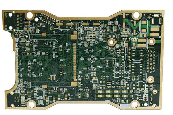
Finally, generating Gerber files (the standard format for PCB fabrication) was the last step. I used online services like JLCPCB and PCBWay for affordable prototypes.
Challenges Faced Along the Way
1. Debugging Errors
My first few designs had mistakes—some obvious, some subtle. A common issue was incorrect footprints, where a component’s physical size didn’t match the PCB pad layout. This taught me to double-check datasheets before finalizing a design.
2. Signal Integrity Problems
In one project, my microcontroller kept resetting unexpectedly. After research, I realized I had neglected decoupling capacitors near the power pins. Adding them fixed the issue.
3. Manufacturing Constraints
Not all PCB manufacturers support the same specifications. Some had limitations on:
- Minimum trace width
- Hole sizes for vias
- Silkscreen clarity
I learned to adjust my designs based on the manufacturer’s capabilities.
Key Takeaways and Advice for Beginners
1. Start Simple
Don’t attempt a complex 4-layer board on your first try. Begin with single-sided or double-sided designs and gradually increase complexity.
2. Learn from Open-Source Projects
Studying existing PCB designs (e.g., Arduino, Raspberry Pi) helped me understand best practices in component placement and routing.
3. Prototype Before Mass Production
Always order a prototype before committing to a large batch. Catching errors early saves time and money.
4. Join Communities
Forums like EEVblog, Reddit’s r/PrintedCircuitBoard, and Stack Exchange were invaluable for troubleshooting and advice.
5. Patience is Key
PCB design is iterative. Mistakes will happen, but each one is a learning opportunity.
Conclusion
Learning PCB design from scratch was a journey filled with trial and error, but the satisfaction of holding a functional board that I designed myself made it all worthwhile. The key to success lies in persistence, continuous learning, and leveraging available resources. Whether you’re a hobbyist or aspiring professional, PCB design is a skill that opens doors to countless innovations in electronics.
If I had to summarize my experience in one sentence: “PCB design is not just about connecting components—it’s about thinking like an engineer, an artist, and a problem-solver all at once.”
For anyone starting this journey, my advice is simple: Take it step by step, embrace mistakes, and keep designing


