Removing PBGA Packages from PCBs
How to remove a plastic ball grid array package (PBGA) from a printed circuit board (PCB) is a skill that every hardware engineer must have. ADI provides a recommended rework procedure for removing PBGA packages from PCBs.
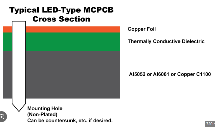
PBGA is a type of package whose main distinguishing feature is the use of an array of solder balls to contact the substrate (such as a PCB). This feature gives PBGA an advantage over other packages with different pin configurations (such as single-row, dual-in-line, and quad-row), which is the ability to achieve higher pin density. The interconnection within the PBGA package is achieved through wire bonding or flip chip technology. The PBGA chip containing the integrated circuit is encapsulated in a plastic encapsulation material.
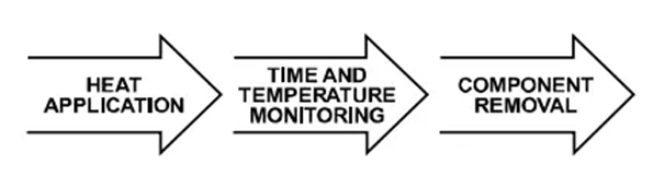
Figure 1. Schematic diagram of PBGA device PBGA device rework After assembling the PBGA device on the PCB, if defects are found, it should be reworked to remove the defective device and replace it with a working device. Before removing the device, the defective device should be heated until the solder joint liquefies to facilitate the removal of the defective device from the circuit board.
The general rework procedure is as follows
❶ Prepare the board
❷ Remove the device
❸ Clean the PCB pads
❹ Apply solder paste
❺ Align and mount the device
❻ Fix the device
❼ Check
Before introducing the above 7 steps in detail, let’s talk about the precautions for removing the device and delamination.
When removing the device, mechanical stress may be generated on the PBGA and/or PCB. Defective devices should be removed carefully to avoid damage to the PCB, adjacent devices, and the defective device itself, especially if the user intends to perform failure analysis on the defective device.
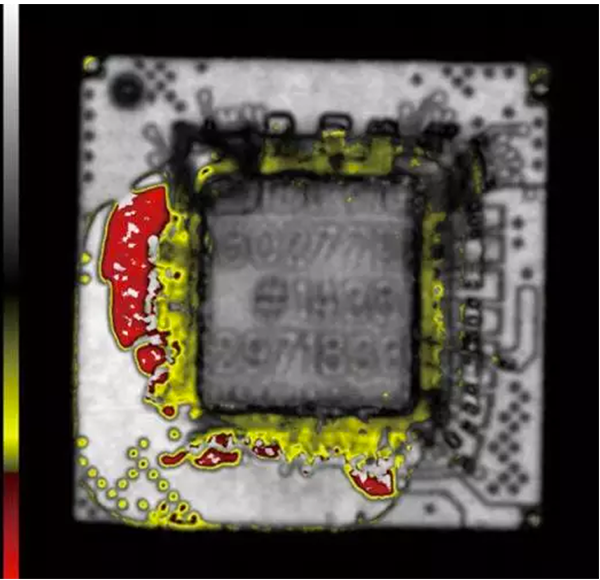
If there is too much stress on the PBGA device, such as heating the device above the rated peak temperature or excessive exposure to high temperature, it may cause package delamination or external physical damage (see Figures 2 and 3). For devices that are to be further analyzed, delamination caused by improper removal will make it more difficult to find the true failure mechanism. Therefore, in order to conduct effective failure analysis, it is necessary to properly remove the defective device.

Figure 2. Overheating causes delamination between the substrate and molding compound of a PBGA device (observed by scanning acoustic microscopy)
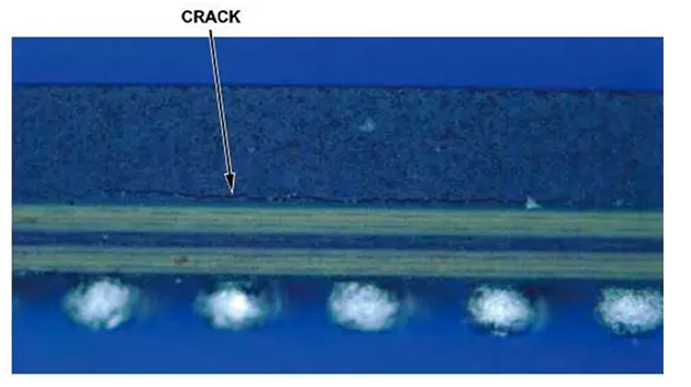
Figure 3. Low magnification image of cracks on a PBGA caused by overheating (side view) Board Preparation
It is strongly recommended that the PCB assembly be dry-baked before rework begins to remove any residual moisture. If not removed, residual moisture may damage the device during reflow due to the “popcorn effect”. Bake the PCB assembly at 125°C for a minimum of 4 hours, as long as these conditions do not exceed the rated limits of other components on the PCB. If these conditions exceed the rated limits of other components, then alternate baking conditions as described in the joint industry standard IPC/JEDEC J-STD-033 should be used.
Device Removal
Different tools can be used to remove the device. To remove the device, the device may be heated until the solder reflows and then removed by mechanical means while the solder is still liquid. Programmable hot air rework systems can provide controlled temperature and time settings. The temperature profile used for the device assembly should be followed during rework. The rework temperature must not exceed the peak temperature specified on the moisture sensitivity level (MSL) label. Heating time can be reduced (e.g. for the liquefaction zone) as long as full solder reflow is achieved. The solder reflow zone should be at peak temperature for less than 60 seconds. The vacuum pressure of the pick-up tool should be less than 0.5 kg/cm2 to prevent the device from being ejected before full reflow is achieved and to avoid pad floating. Do not reuse the device removed from the PCB.
Control the rework temperature to avoid damaging the PBGA device and the PCB. Consider that the PBGA may heat faster than leadframe-based packages such as standard outline integrated circuits (SOICs) and leadframe chip scale packages (LFCSPs) due to the difference in thermal mass. Note that covering the area around the device with heat-resistant tape can provide further protection. In addition, it is recommended to heat the underside of the PCB to reduce the temperature difference between the upper and lower sides of the PCB to minimize board bowing.
When defining the rework tool settings, the temperature profile should be calibrated. This calibration is especially important when reworking a specific device for the first time. PBGA devices also need to be calibrated with different body sizes, solder compositions, or different PCB materials, configurations, sizes, and thicknesses because they may have different thermal mass values.
The calibration must include monitoring of temperature, time, and other settings of the equipment tool (see Figure 4). Thermocouples should be mounted to different parts of the board assembly, such as the top of the PBGA device and the top of the PCB (see Figure 5). Analyze the time and temperature profile data to obtain valid parameters for device removal from the evaluation.
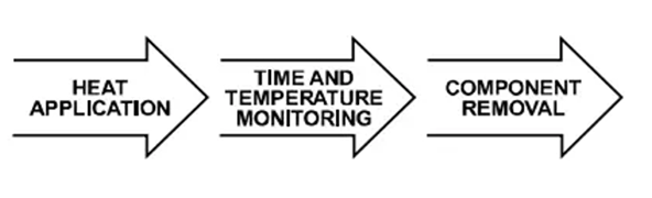
Figure 4. Simplified flowchart for device removal evaluation
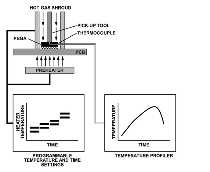
Figure 5. Schematic diagram of device removal calibration setup Cleaning PCB pads
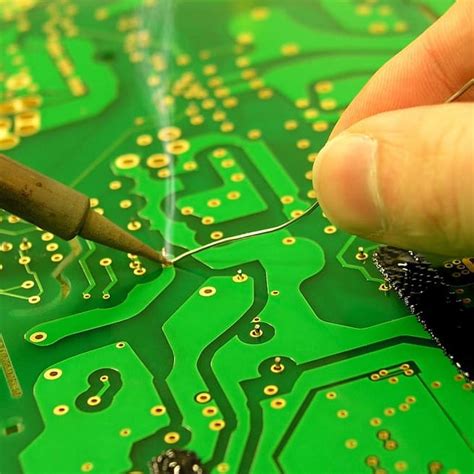
After removing the PBGA device, the pads on the PCB will have excess solder and must be cleaned before installing the replacement PBGA device. Pad cleaning can be divided into two steps:
Desoldering. Remove excess solder from the pads using solder wick and a blade-type soldering iron (see Figure 6). The width of the selected blade should match the maximum width occupied by the device. The blade temperature must be low enough to avoid damaging the board. Flux can be applied to the pads and then excess solder can be removed using solder wick and a soldering iron.
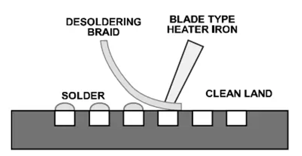
Figure 6. PCB pad desoldering.
Clean the reworked area with a cleaning agent and wipe clean with a lint-free cloth. The cleaning agent used depends on the type of solder paste used in the original assembly.
Applying Solder Paste
Solder paste should be applied before mounting the replacement PBGA device on the board. The purpose is to replace the solder paste applied when the board was originally assembled to ensure the reliability of the PBGA solder joint. The amount of solder paste applied to each solder ball must be consistent to avoid non-coplanarity problems when the PBGA is mounted on the board.
Stencils can be used to apply solder paste to the PCB pads. Stencil alignment accuracy is critical to maintain a uniform reflow soldering process. Use the same PBGA aperture geometry and stencil thickness as the board assembly. Use a trapezoidal aperture (see Figure 7) to ensure uniform solder paste release and reduce smearing.
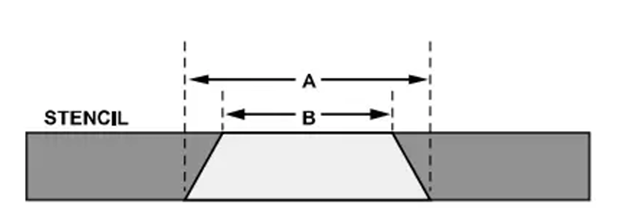
Figure 7. Stencil Aperture Geometry (A is longer than B)In some cases
it may not be feasible to use a stencil to apply solder paste uniformly and accurately to the PCB pads, especially for boards with high device density or tight geometric space. In this case, consider applying solder paste to the solder balls on the bottom of the device. This can be done by using a stencil to apply solder paste to the top of the solder balls or by dispensing solder paste to all solder balls (see Figures 8 and 9). This can be achieved using specially designed fixtures and/or rework equipment.
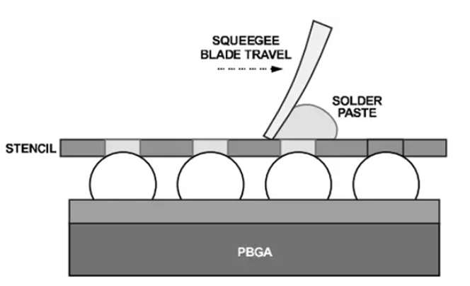
Figure 8. Solder paste stencil applies solder paste to solder balls
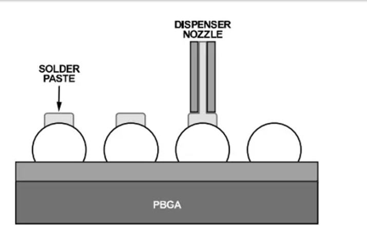
Figure 9. Dispensing solder paste onto solder balls Device alignment and placement
It is important to accurately place the device on the board. Placement equipment with split beam optics can help align the PBGA and board. This type of imaging system involves superimposing a mirror image of the PBGA solder balls on a mirror image of the PCB pads (see Figure 10). The placement machine must have the ability to allow the user to make fine adjustments along the x- and y-axes, including rotation.
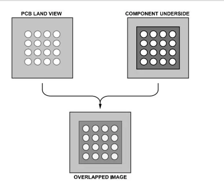
Figure 10. Aligning the PCB and device using split beam optics Placement accuracy depends on the equipment or process used.
Although PBGA packages tend to automatically align during the reflow process, it is important to ensure that the placement deviation is less than 50% of the PCB pad width. If the alignment error is too large, solder bridging may cause electrical shorts. Fixing the device
Because all reflow parameters are optimized, the thermal profile developed during the original assembly process should be used.
Inspection
After reflow, inspect the assembled PBGA for defects such as misalignment or damage. Use X-ray to check for problems such as solder bridging and solder beads. If necessary, perform electrical verification tests to verify that the device is functioning properly.
Bingo, that’s it for the rework procedure of removing the PBGA package from the PCB!