Restore the circuit diagram according to the PCB board
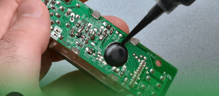
Schematic diagram production is the basis of PCB layout, so the schematic diagram restoration should be completed without errors. There should be no errors in the schematic design, and it must be cross-checked by another MCU development engineer to evaluate any errors in the design. Otherwise, the wrong schematic will be converted to the PCB and cause the PCB to not operate as expected. When encountering some small objects, or encountering electronic products without drawings, it is necessary to draw the circuit schematic according to the real object.
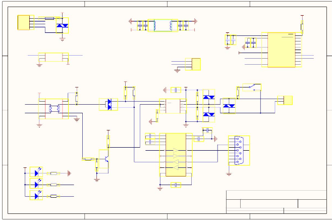
There are 8 ways to restore the PCB schematic according to the PCB board:
- Select electronic components such as integrated circuits, transformers, transistors, etc. that are large in size, have many pins, and play a major role in the circuit, and then extract them from the selected reference pins to reduce errors.
- If the PCB is marked with component numbers (such as VD870, R330, C466, etc.), since these serial numbers have specific rules, components with the same Arabic numerals after English letters are the same functional units, so drawings should be used. Correctly distinguishing components of the same functional unit is the basis for drawing PCB layout.
- If there is no serial number of the component marked on the printed circuit board, it is best to number the component yourself for easy analysis and proofreading. When designing printed circuit board components, manufacturers generally arrange the components of the same functional unit relatively to minimize copper foil routing. Once a device with core functions is found, as long as it can be found, other components of the same functional unit can be found.
- Correctly distinguish the ground wire, power line and signal line of the printed circuit board. Taking the power supply circuit as an example, the negative pole of the rectifier connected to the secondary of the power transformer is the positive pole of the power supply. A large-capacity filter capacitor is generally connected between the ground and the ground, and the capacitor shell has a polarity mark. The power line and ground line can also be found from the three-terminal regulator pin. When the factory is wiring the printed circuit board, in order to prevent self-excitation and anti-interference, the grounding copper foil is generally set to the widest (high-frequency circuits often have large-area grounding copper foil), followed by the power copper foil, and the signal copper foil is the narrowest. In addition, in electronic products with both analog circuits and digital circuits, the printed circuit board often separates its ground wire to form an independent grounding network, which can also be used as a basis for identification and judgment.
- To avoid too much wiring of components, the wiring of the circuit diagram is crisscrossed, causing the picture to be messy. Terminal markings and grounding symbols can be used extensively for power lines and ground lines. If there are many components, unit circuits can be drawn separately and then combined.
- When drawing sketches, it is recommended to use transparent tracing paper and use colored pens to draw ground lines, power lines, signal lines, components, etc. according to color. When modifying, gradually deepen the color to make the drawing visually eye-catching and facilitate circuit analysis.
- Master the basic composition and classic drawing methods of some unit circuits, such as rectifier bridges, voltage regulator circuits and op amps, digital integrated circuits, etc. These unit circuits are directly drawn to form the framework of the circuit diagram, which can improve the drawing efficiency.
- When drawing a circuit diagram, try to find the circuit diagram of similar products as a reference to get twice the result with half the effort.