Reverse Engineering PCB Boards: Techniques, Tools, and Ethical Considerations
Introduction
Printed Circuit Board (PCB) reverse engineering is a complex but increasingly valuable skill in electronics design, cybersecurity, and hardware analysis. This process involves deconstructing an existing PCB to understand its architecture, components, and functionality without access to original design documents. As technology continues to advance at a rapid pace, the ability to analyze and learn from existing designs has become crucial for innovation, security testing, and legacy system maintenance.
This comprehensive guide explores the methodologies, tools, challenges, and ethical considerations involved in PCB reverse engineering. Whether you’re an electronics enthusiast, a security researcher, or an engineer working with legacy systems, understanding these techniques can provide valuable insights into hardware design and functionality.
Understanding PCB Reverse Engineering
Definition and Purpose
PCB reverse engineering refers to the process of analyzing a manufactured circuit board to extract information about its design, components, and functionality. Unlike traditional engineering that progresses from concept to product, reverse engineering works backward from the physical product to uncover the original design intent.
Common applications include:
- Recovering lost design documentation for legacy systems
- Analyzing competitor products for research and development
- Identifying security vulnerabilities in hardware
- Repairing or modifying systems when original documentation is unavailable
- Detecting counterfeit components or intellectual property theft
- Educational purposes to understand advanced circuit designs
Legal and Ethical Considerations
Before beginning any reverse engineering project, it’s crucial to consider the legal and ethical implications:
- Intellectual Property Laws: Many countries have specific laws governing reverse engineering. In the United States, the Digital Millennium Copyright Act (DMCA) includes provisions that may affect reverse engineering activities.
- End User License Agreements (EULAs): Some products explicitly prohibit reverse engineering in their terms of service.
- Ethical Use: Even when legal, consider whether your activities could compromise security systems or violate privacy.
- Documentation: Maintain clear records of your process to demonstrate legitimate purposes if questioned.
Always consult with legal professionals when working with commercial products or systems you don’t own
The Reverse Engineering Process
Step 1: Preparation and Documentation
- Gather Tools: Prepare all necessary equipment including multimeters, oscilloscopes, soldering equipment, and imaging devices.
- Create a Workspace: Establish a clean, well-lit area with proper ESD (electrostatic discharge) protection.
- Initial Documentation:
- Photograph the board from multiple angles
- Note all visible markings, logos, and identifiers
- Record dimensions and layer count (if visible)
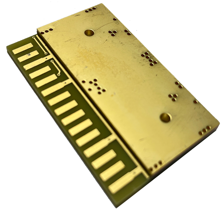
Step 2: Non-Destructive Analysis
Before any physical intervention, conduct thorough non-invasive examination:
- Visual Inspection:
- Identify all major components (ICs, connectors, large passives)
- Note component markings and package types
- Look for test points or debugging interfaces
- Power Analysis:
- Identify power inputs and measure voltages
- Map power distribution networks
- Note any voltage regulators and their configurations
- Connectivity Mapping:
- Use a multimeter in continuity mode to trace obvious connections
- Identify ground planes and common nets
Step 3: Component Identification
- IC Identification:
- Research markings using datasheet databases
- Note package types and pin counts
- For proprietary chips, document all available information
- Passive Components:
- Measure resistors and capacitors where possible
- Note inductor values and types
- Document component placement and orientation
- Specialized Components:
- Identify crystals and oscillators
- Note any RF components or antennas
- Document connectors and interface types
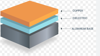
Step 4: Board Imaging and Layer Analysis
For multi-layer boards, more advanced techniques are required:
- X-ray Imaging:
- Reveals internal layers and via structures
- Helps identify buried components
- Requires specialized (and often expensive) equipment
- Layer Delamination:
- Carefully sand or chemically remove layers
- Destructive method that requires extreme caution
- Only recommended when absolutely necessary
- Optical Scanning:
- High-resolution scans of each layer
- Can be processed with image analysis software
Step 5: Schematic Recreation
Using collected data, reconstruct the circuit schematic:
- Netlist Generation:
- Create a list of all electrical connections
- Group related circuits functionally
- Schematic Capture:
- Use EDA (Electronic Design Automation) tools
- Organize circuits logically (power, digital, analog, etc.)
- Add component values and references
- Verification:
- Cross-check connections with physical board
- Test critical paths with measurement tools
- Look for inconsistencies or missed connections
Step 6: Functional Analysis
With schematic complete, analyze circuit operation:
- Block Diagram Creation:
- Identify major functional blocks
- Understand signal flow and processing
- Signal Analysis:
- Use oscilloscopes or logic analyzers
- Capture timing and signal integrity data
- Firmware Extraction (if applicable):
- Dump contents of programmable devices
- Analyze code for additional insights

Tools for PCB Reverse Engineering
Hardware Tools
- Basic Equipment:
- Digital multimeter
- Soldering/desoldering station
- Magnification tools (microscope or loupe)
- Advanced Tools:
- Oscilloscope (preferably digital)
- Logic analyzer
- X-ray inspection system
- Thermal imaging camera
- Specialized Tools:
- JTAG/SWD debuggers
- Chip programmers
- Bus pirates or protocol analyzers
Software Tools
- Image Processing:
- GIMP or Photoshop for board image enhancement
- OpenCV for automated trace recognition
- EDA Software:
- KiCad (open-source)
- Altium Designer (commercial)
- Eagle (now Fusion 360)
- Analysis Tools:
- IDA Pro for firmware analysis
- Sigrok for signal decoding
- Binary analysis frameworks like Ghidra
Challenges in PCB Reverse Engineering
Technical Challenges
- High-Density Designs:
- Fine-pitch components and microvias
- Multi-layer boards with buried/blind vias
- Miniaturized components (0201 or smaller)
- Advanced Packaging:
- System-in-Package (SiP) designs
- Chip-on-Board (COB) implementations
- Flip-chip and wafer-level packaging
- Protection Mechanisms:
- Encrypted or locked microcontrollers
- Tamper-proof coatings
- Obfuscated or erased markings
Methodological Challenges
- Time Consumption:
- Complex boards may require hundreds of hours
- Verification process can be iterative
- Accuracy Verification:
- Ensuring no connections are missed
- Validating assumptions about circuit operation
- Component Availability:
- Obsolete or proprietary components
- Custom ASICs with no public documentation
Advanced Techniques
Non-Invasive Methods
- Power Analysis Attacks:
- Monitoring power consumption to infer operations
- Particularly relevant for cryptographic systems
- Electromagnetic Analysis:
- Using near-field probes to detect EM emissions
- Can reveal clock signals and data patterns
- Fault Injection:
- Glitch attacks to disrupt normal operation
- Can bypass security measures in some cases
Invasive Methods
- Depackaging ICs:
- Chemical or mechanical removal of packaging
- Allows die inspection and microprobing
- Focused Ion Beam (FIB):
- Ultra-precise circuit modification
- Requires specialized equipment
- Scanning Electron Microscopy:
- High-resolution imaging of chip structures
- Can reveal ROM contents in some cases
Ethical Reverse Engineering Practices
To ensure your work remains ethical and legal:
- Only Reverse Engineer What You Own: Work only on boards you have legal rights to analyze.
- Respect Intellectual Property: Use gained knowledge for legitimate purposes, not cloning.
- Responsible Disclosure: If finding vulnerabilities, follow proper disclosure protocols.
- Educational Focus: Use skills to learn and innovate, not to infringe on others’ work.
- Document Everything: Maintain clear records of your process and intentions.
Applications of PCB Reverse Engineering
Positive Use Cases
- Legacy System Maintenance:
- Supporting old industrial equipment
- Military system sustainment
- Security Research:
- Hardware vulnerability discovery
- Tamper-proofing analysis
- Educational Purposes:
- Learning from quality designs
- Understanding advanced techniques
- Interoperability Development:
- Creating compatible systems
- Developing drivers for undocumented hardware
Controversial Applications
- Competitive Intelligence:
- While legal in some cases, may violate ethical boundaries
- Counterfeit Production:
- Illegal cloning of products
- Violates numerous intellectual property laws
- Malicious Hardware Modification:
- Creating compromised versions of systems
- Hardware backdoor implantation
Future Trends in PCB Reverse Engineering
- Automation and AI:
- Machine learning for trace recognition
- Automated component identification
- Advanced Imaging Techniques:
- Improved X-ray tomography
- Terahertz imaging for non-destructive analysis
- Increased Security Measures:
- More sophisticated anti-RE techniques
- Active tamper detection circuits
- Cloud-Based Tools:
- Collaborative reverse engineering platforms
- Shared component databases
Conclusion
PCB reverse engineering is a powerful skill that combines technical knowledge, analytical thinking, and meticulous attention to detail. While the process can be challenging, particularly with modern high-density designs, the insights gained can be invaluable for security research, legacy system support, and technical education.
As with any powerful capability, reverse engineering comes with significant ethical responsibilities. Practitioners must always consider the legal implications of their work and strive to use these techniques for positive, constructive purposes.
The field continues to evolve alongside electronic design technologies, with new tools and methodologies emerging to address increasingly complex PCB designs. Whether you’re approaching reverse engineering as a professional requirement or a personal challenge, maintaining up-to-date knowledge of both technical processes and legal frameworks is essential for successful and responsible practice.