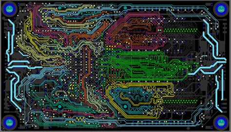
Revisiting the Major Evolutionary Paths of Power PCB Structures
Introduction
Printed Circuit Boards (PCBs) have served as the backbone of electronic systems for decades, with their power delivery structures undergoing significant transformations to meet the ever-increasing demands of modern electronics. This article traces the evolutionary journey of power PCB structures, examining how technological advancements, material innovations, and changing application requirements have shaped their development. From simple single-layer designs to sophisticated multilayer architectures with embedded components, power PCB structures have continuously evolved to address challenges in power integrity, thermal management, and miniaturization.
1. The Early Era: Single-Layer Power Distribution (1950s-1970s)
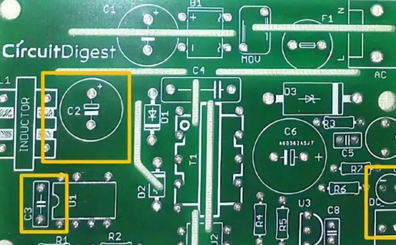
The genesis of power PCB structures can be traced back to the mid-20th century when electronic systems first began transitioning from point-to-point wiring to printed circuit boards. These early power PCBs featured:
Basic Single-Layer Designs: The simplest implementations used a single conductive layer for both power distribution and signal routing, with jumpers providing interconnections where needed. Power and ground were often routed as simple traces alongside signal lines.
Bus Bar Architectures: Some early designs incorporated copper bus bars either as part of the PCB or as separate mechanical components attached to the board. These provided low-impedance power distribution but limited design flexibility.
Discrete Decoupling: Bulk capacitors were placed near power-hungry components, but without sophisticated decoupling strategies. The concept of power integrity was in its infancy, and designs often suffered from significant noise and voltage fluctuations.
Material Limitations: Early PCB materials like SRBP (Synthetic Resin Bonded Paper) and FR-2 (Flame Retardant 2) had poor thermal and electrical characteristics compared to modern standards, limiting power delivery performance.
2. The Revolution: Introduction of Dedicated Power Planes (1980s)
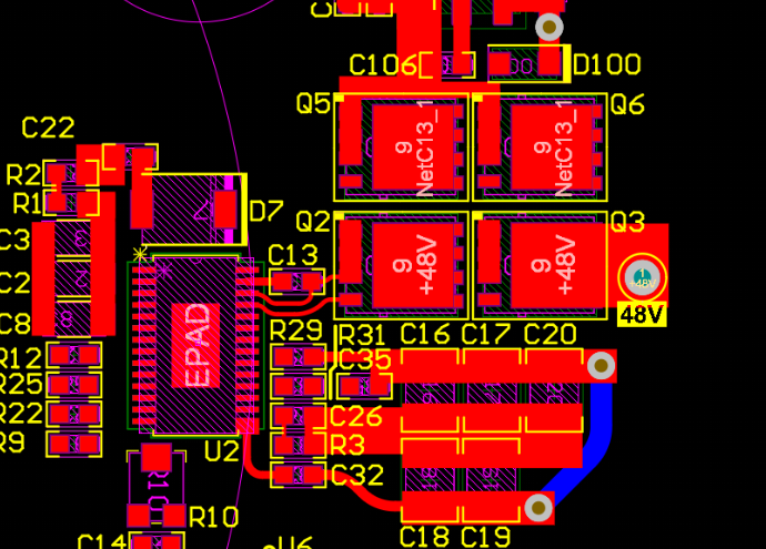
The 1980s marked a significant turning point in power PCB evolution with the widespread adoption of multilayer boards and dedicated power planes:
Dedicated Power and Ground Planes: The introduction of separate layers exclusively for power and ground distribution represented a quantum leap in power delivery performance. These continuous copper planes provided:
- Lower impedance power distribution
- Improved noise immunity
- Better current carrying capacity
- Reduced electromagnetic interference (EMI)
Decoupling Strategies: The use of power planes enabled more effective decoupling capacitor placement and the development of comprehensive power distribution networks (PDNs). Engineers began understanding the importance of minimizing loop inductance in high-speed circuits.
Material Advancements: The transition to FR-4 (Flame Retardant 4) as the standard PCB material provided better thermal stability and electrical properties, supporting more reliable power delivery.
Impedance Control: As signal speeds increased, the power plane structure became integral to controlled impedance routing, with the power-ground plane pair serving as a reference for critical signals.
3. The High-Speed Era: Power Integrity Optimization (1990s-2000s)
The 1990s and early 2000s saw exponential growth in clock frequencies and power demands, driving significant innovations:
Split Power Planes: Designers began partitioning power planes to accommodate multiple voltage rails required by complex ICs. Careful attention was paid to plane splits to minimize impedance discontinuities.
Buried Capacitance: The development of buried capacitance materials (such as ZBC® from Zycon) allowed for distributed decoupling directly within the PCB stackup, reducing the need for discrete capacitors.
High-Density Interconnect (HDI): The adoption of microvias and finer features enabled more compact power distribution networks while maintaining performance.
Advanced Simulation Tools: The emergence of sophisticated power integrity analysis tools allowed designers to model and optimize power delivery networks before fabrication.
Power Island Architectures: Some designs implemented localized power regions with different characteristics optimized for specific circuits or components.
4. The Modern Era: 3D Integration and Advanced Materials (2010-Present)
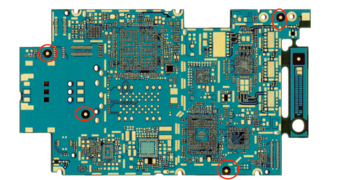
Recent years have witnessed revolutionary approaches to power PCB structures:
Embedded Power Components: Active and passive power components are now routinely embedded within the PCB layers, including:
- Embedded discrete capacitors
- Buried voltage regulators
- Integrated magnetics for power conversion
3D Power Delivery: Stacked die and package-on-package (PoP) technologies have driven the development of through-silicon vias (TSVs) and other 3D interconnection methods for power distribution.
Advanced Materials: New materials have emerged to address modern challenges:
- High-thermal-conductivity substrates for improved heat dissipation
- Low-loss dielectrics for high-frequency power delivery
- Stretchable/flexible conductors for wearable electronics
Power Via Optimization: Sophisticated via structures have been developed to minimize impedance in power delivery networks:
- Staggered via patterns
- Via-in-pad technologies
- Solid via bars for high-current applications
Active Power Planes: Some cutting-edge designs incorporate active circuitry within the power plane structure itself, blurring the line between PCB and integrated circuit.
5. Emerging Trends and Future Directions
The evolution of power PCB structures continues unabated, with several promising directions:
Substrate Integrated Power: The integration of complete power conversion and management systems within the PCB substrate.
Graphene and 2D Materials: Exploration of novel conductive materials offering superior thermal and electrical properties.
Photonic Power Delivery: Investigation of optical power transmission within PCBs for specific applications.
AI-Optimized Power Structures: Use of machine learning algorithms to generate optimized power distribution patterns tailored to specific applications.
Sustainable Power PCBs: Development of eco-friendly power delivery structures using biodegradable materials and low-energy manufacturing processes.
Conclusion
The evolution of power PCB structures reflects the broader trajectory of electronic systems – from simple implementations to highly sophisticated, optimized solutions. Each evolutionary step has addressed the limitations of previous approaches while introducing new capabilities. As electronic systems continue to push boundaries in performance, miniaturization, and functionality, power PCB structures will undoubtedly continue their remarkable evolution. Understanding this historical progression provides valuable insights for tackling current design challenges and anticipating future requirements in power delivery systems.
The journey from basic single-layer boards to today’s 3D-integrated power delivery networks demonstrates the remarkable innovation that has occurred in this often-overlooked aspect of electronic design. As we look to the future, the continued evolution of power PCB structures will play a critical role in enabling next-generation electronic systems across all application domains.

