Revolutionizing Electronics: The Future of Additive PCB Manufacturing
Key Takeaways
As you delve into the realm of additive PCB manufacturing, understanding its implications and advantages is essential for anyone involved in pcb manufacturing or related industries. This innovative approach significantly alters the landscape of traditional pcb manufacturing by enabling increased design flexibility and efficiency. With the integration of 3D printing technology, you can witness a notable reduction in pcb manufacturing cost, which is a major consideration for pcb manufacturing companies and entrepreneurs alike. By embracing these advanced techniques, you are not only streamlining your production processes but also optimizing the overall workflow within your pcb manufacturing business. This paradigm shift allows for rapid iterations during prototyping, empowering you to transform ideas into tangible products faster than ever before. Furthermore, the ability to produce complex geometries that were once thought impossible opens new avenues for creativity and innovation in electronic design. Overall, recognizing these takeaways can greatly enhance your strategic approach towards adopting additive methodologies in your operations.
Understanding Additive PCB Manufacturing: An Overview
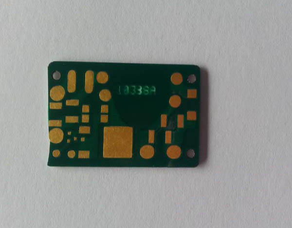
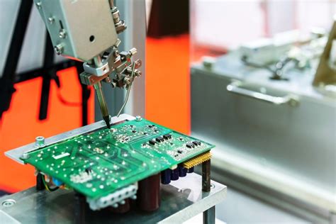
Additive PCB manufacturing is at the forefront of modern electronics production, offering a revolutionary approach compared to traditional methods. In this technique, layers of material are added to create intricate printed circuit boards (PCBs) that cater to specific design requirements. This process not only streamlines production but also reduces the pcb manufacturing cost, making it an attractive option for both established pcb manufacturing companies and emerging pcb manufacturing businesses.
One of the standout features of additive PCB manufacturing is its remarkable ability to enhance design flexibility. With traditional methods, you often face limitations due to the complexity of assembly and component placement. However, additive techniques allow for more complex geometries and designs that were previously infeasible or costly to achieve. For instance, you can integrate multiple components directly into the layer structure rather than assembling them separately, thus minimizing errors and improving overall efficiency.
As you delve deeper into this technology, you’ll uncover various applications across different industries. The combination of cost-effectiveness, design adaptability, and steadily reduced lead times positions additive PCB manufacturing as a pivotal component in the future of electronics production. With numerous pcb manufacturing companies adopting these practices, you can expect a significant shift in how products are developed and brought to market.
| Feature | Traditional Manufacturing | Additive Manufacturing |
|---|---|---|
| Design Complexity | Limited | High |
| Production Lead Time | Longer | Shorter |
| Cost Effectiveness | Variable | Generally Lower |
| Material Waste | Higher | Lower |
In conclusion, understanding additive PCB manufacturing is essential for grasping how it reshapes the landscape of electronics production today and in the years to come. If you’re interested in exploring more about this innovative field, consider checking out Andwin PCB.
Key Advantages of Additive PCB Manufacturing
Additive PCB manufacturing is poised to significantly change the landscape of PCB manufacturing. By leveraging 3D printing techniques, this approach offers design flexibility that traditional methods simply cannot match. Imagine being able to create complex structures and geometries that were once deemed impossible, all while keeping your PCB manufacturing cost under control. This flexibility allows for rapid iterations in design, enabling you to tailor your products to meet specific requirements without the burdensome costs typically associated with conventional PCB manufacturing companies. Moreover, the quick turn-around times associated with additive processes mean that your ideas can transition from concept to prototype in a fraction of the time, helping you stay ahead in a fast-paced marketplace where reducing lead times is crucial. The ability to combine different materials seamlessly also enhances the overall functionality of your products, making them more competitive. Overall, additive PCB manufacturing is not just a passing trend; it represents a significant shift in how you can operate your PCB manufacturing business, positioning you for success in an ever-evolving technological landscape.
Cost Savings Through Additive PCB Techniques
In the landscape of pcb manufacturing, one of the most compelling advantages of adopting additive techniques lies in the significant cost savings they offer. By leveraging technologies such as 3D printing, businesses can drastically reduce the pcb manufacturing cost associated with traditional methods. You may find that fewer materials are wasted, as additive processes build up layers of material only where necessary, unlike subtractive methods that often leave a considerable amount of scrap. This efficiency is particularly beneficial for small batch productions or prototyping, where traditional pcb manufacturing companies may charge a premium for low-volume orders.
Moreover, the need for complex tooling is diminished with additive techniques, allowing you to minimize the expenses tied to mold creation and setup fees. This means that even small pcb manufacturing business operations can scale up their production capabilities without incurring exorbitant upfront costs. As you explore options in additive manufacturing, remember that these technologies not only facilitate cost-effective production but also enable faster iteration cycles, allowing you to bring your designs to market rapidly and with greater precision.
“Embracing additive PCB techniques is not just about cutting costs; it’s about redefining what’s possible in electronic design and production.”
With these advantages in mind, you can stay ahead in an ever-competitive market by implementing strategies that prioritize both economic efficiency and innovative potential within your pcb manufacturing processes.
Enhancing Design Flexibility in Electronics with 3D Printing
Additive PCB manufacturing is at the forefront of a new era in electronics design, significantly improving the way you approach creating circuit boards. One of the primary benefits of this technology is its unmatched design flexibility. Traditional methods often impose limitations on how intricate and compact designs can be, primarily due to the rigid processes involved. However, with 3D printing techniques, your ability to innovate expands dramatically; you’re no longer constrained by established norms. This freedom allows for intricate geometries and unique layouts that traditional PCB manufacturing companies may struggle to replicate.
In addition to design flexibility, these advancements impact your overall PCB manufacturing cost. By utilizing additive methods, you can reduce material waste and labor costs associated with conventional production techniques. This means that your PCB manufacturing business can not only create more complex designs but also do so in a more economical manner, optimizing your budget without compromising quality. As a result, adding custom features and adapting designs becomes simpler; you can iterate rapidly based on client needs or project demands without incurring significant extra expenses or lead times.
Ultimately, embracing additive processes means embracing a future where your design choices are limited only by your imagination rather than by manufacturing constraints. With these exciting developments in additive PCB manufacturing, you’ll find yourself well-equipped to push the boundaries of electronic innovation, leading the way into a more flexible and efficient production landscape.
Reducing Lead Times: The Speed of Additive Manufacturing
In the dynamic world of PCB manufacturing, you are likely aware of the challenges posed by traditional methods, particularly when it comes to lead times. However, with additive PCB manufacturing, those challenges are significantly diminished. This innovative approach allows for rapid prototyping and production, streamlining processes that once took weeks or even months. By leveraging 3D printing technologies, PCB manufacturing companies can produce complex designs swiftly, facilitating faster iterations and reducing time-to-market. As a result, you will find yourself able to respond promptly to market demands, adjusting designs as needed without incurring substantial delays or additional costs. This decrease in lead times is not just a matter of efficiency; it also contributes to more sustainable practices in the PCB manufacturing business, ultimately enhancing your competitive edge. With the ability to complete projects in less time and at reduced costs, your organization can focus more on innovation rather than getting bogged down by prolonged production schedules. By embracing these advancements in additive manufacturing, you open doors to a realm where speed and flexibility redefine the possibilities within the electronics landscape.
Transforming Prototyping Processes with Additive Technologies
In today’s fast-paced technological landscape, additive PCB manufacturing is revolutionizing the way you approach prototyping. Traditionally, the prototyping process often involves long lead times and substantial pcb manufacturing costs. However, with the advent of additive technologies, you can streamline your workflow and significantly enhance efficiency. Instead of relying solely on conventional methods, which may limit your design capabilities, you can harness the power of 3D printing to create complex designs that were once deemed impractical. By utilizing these technologies, pcb manufacturing companies can cater to a wider array of specifications and customizations as they develop new products. This not only boosts creativity in your projects but also allows you to iterate designs faster than ever before. Consequently, the agility in prototyping made possible by additive PCB manufacturing positions your pcb manufacturing business to respond more effectively to market demands while keeping pcb manufacturing costs at a minimal level. The result is a more adaptable production process that transforms ideas into tangible products in record time, paving the way for future innovations in electronic design and fabrication.
Real-World Applications of Additive PCB Manufacturing
Additive PCB manufacturing is making significant strides across various industries, allowing for innovative solutions that were previously unimaginable. In the electronics sector, companies are increasingly turning to additive methods to meet their design needs effectively and efficiently. For instance, pcb manufacturing companies are now utilizing 3D printing techniques to create custom circuit boards that cater to specific project requirements. This level of customization offers unparalleled design freedom, enabling you to experiment with complex geometries and integrate multiple functionalities into a single board. Furthermore, the cost-effectiveness of pcb manufacturing cost has become a notable aspect, particularly for small-scale producers or startups aiming to minimize their upfront investments while maximizing productivity. Industries such as automotive and aerospace are also seeing benefits in their pcb manufacturing business, as additive techniques facilitate rapid prototyping and lower lead times. By leveraging this transformational technology, you can stay ahead in a competitive market and meet the ever-evolving demands of your customers effectively. The ability to quickly produce prototypes means you can test design iterations faster than ever before, bringing products to market with unprecedented speed and efficiency.
The Future of Electronics: Trends in Additive PCB Production
As you consider the evolution of PCB manufacturing, it’s essential to familiarize yourself with how additive technologies are poised to reshape the landscape. The shift towards additive PCB manufacturing represents a significant trend that merges advanced technology with modern production techniques. This innovative approach not only emphasizes the reduction of PCB manufacturing costs but also enhances the efficiency and scope of design possibilities. With your interest in staying ahead, understanding how PCB manufacturing companies are integrating 3D printing and other additive methods could be crucial for your business strategy. The ability to create complex geometries and incorporate multiple functionalities directly into your circuit boards will transform how you perceive prototyping and production timelines. This evolution ultimately redefines your expectations as a stakeholder in the PCB manufacturing business, inviting you to explore methods that are not just innovative but also pragmatic in addressing current market demands. Embracing these trends positions you at the forefront of an industry that is rapidly approaching a new era of efficiency and capability, suggesting that the future of electronics may very well be molded by additive PCB manufacturing practices that prioritize cost-effectiveness and design agility.
Conclusion
As you navigate the evolving landscape of pcb manufacturing, it’s essential to recognize the significant advancements that additive PCB manufacturing brings to the table. This innovative approach not only addresses many of the traditional challenges faced by pcb manufacturing companies but also opens new avenues for creativity and efficiency. By embracing this technology, you can benefit from considerable cost savings, which is a crucial factor for any pcb manufacturing business aiming to remain competitive in today’s market. The flexibility inherent in additive processes allows for intricate designs that were once thought impractical, enabling you to push the boundaries of what is possible in electronics. Moreover, with reduced lead times, your projects can move from concept to reality faster than ever before. As such, understanding and leveraging additive PCB manufacturing will be vital for your continued success in this dynamic industry. Whether you are exploring new product designs or seeking to optimize your existing processes, the transformative potential of this technology will undoubtedly play a pivotal role in shaping the future of electronic prototyping and production.
FAQs
What is additive PCB manufacturing?
Additive PCB manufacturing refers to a process that builds printed circuit boards (PCBs) layer by layer using 3D printing technologies. This approach contrasts with traditional subtracting methods, offering a more innovative way to produce complex electronic structures.
What are the key benefits of using additive PCB manufacturing?
The primary advantages include design flexibility, significant cost savings, and reduced lead times for production. This technology allows for intricate designs that are often impossible or too costly to achieve with traditional methods, benefiting both small-scale designs and large enterprises alike.
How does additive PCB manufacturing lower costs?
By utilizing additive techniques, you can reduce material waste since the process only uses the material required for each layer. This not only lowers PCB manufacturing cost, but also enhances the sustainability of production practices.
Are there specific PCB manufacturing companies leading in this area?
Yes, numerous PCB manufacturing companies specialize in additive processes. These companies focus on leveraging innovative technologies that enhance product quality while reducing time-to-market and overall costs.
What is the impact of this technology on prototyping?
Additive manufacturing speeds up the prototyping process significantly. You can quickly iterate on designs and produce functional prototypes without the delays commonly associated with traditional PCB manufacturing methods.
For more detailed insights and information about PCB manufacturing, please click here: Andwin PCB Manufacturing