Revolutionizing Electronics: The Rise of Additive PCB Manufacturing
Key Takeaways
Additive PCB manufacturing is paving the way for a transformative shift in the electronics industry. One of the most significant aspects is the ability to enhance design flexibility, allowing you to create intricate layouts and complex circuit designs that were previously difficult or impossible with traditional methods. This innovation enables PCB manufacturing companies to quickly adapt to market demands, facilitating faster product iterations and shorter time-to-market cycles. In addition, the integration of additive techniques into PCB manufacturing processes significantly reduces PCB manufacturing costs by minimizing waste material and streamlining production workflows. As a result, your business can benefit not only from economic savings but also from enhanced competitiveness in an ever-evolving marketplace. This shift embraces advances in technology such as 3D printing, which empowers manufacturers to produce prototypes and final products with unprecedented speed and efficiency. Consequently, whether you are considering starting a PCB manufacturing business or seeking to improve existing operations, understanding these key takeaways can illuminate how additive methods are revolutionizing the field while providing strategic advantages that can lead to substantial growth and innovation.
Introduction to Additive PCB Manufacturing: An Overview
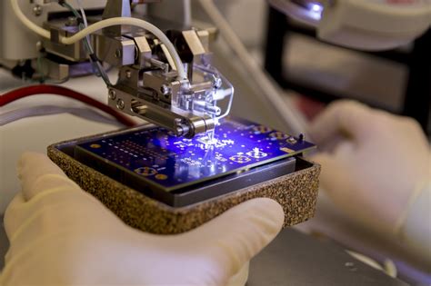
In recent years, additive PCB manufacturing has emerged as a game changer in the electronics industry. You may find this innovative approach particularly appealing as it can significantly enhance your design capabilities. By utilizing additive manufacturing techniques, PCB manufacturing companies are able to streamline the production process and create complex circuit structures that were once deemed impractical. This shift is not only beneficial for custom designs but also leads to a reduction in PCB manufacturing costs. As you explore the nuances of this technology, you’ll discover how it facilitates rapid prototyping, allowing for faster iterations and testing phases in your projects.
Moreover, this method enables a higher degree of customization, catering to specific client needs while minimizing material waste. Companies engaged in the PCB manufacturing business are increasingly adopting these techniques to remain competitive in a rapidly evolving market. As you navigate this exciting landscape, consider the potential advantages of additive PCB methods for enhancing efficiency and driving innovation within your own projects.
“Embrace change and leverage new technologies for better product outcomes.”
This insight serves as a reminder that adapting to evolving practices like additive manufacturing can position you at the forefront of technological advancement in electronics.
Benefits of Additive PCB Manufacturing in Electronics
The shift towards additive PCB manufacturing is fundamentally transforming the landscape of your electronics production. This innovative approach allows you to produce printed circuit boards with unparalleled flexibility, enabling pcb manufacturing companies to create intricate designs that were once deemed impractical or too costly. One major advantage is the reduction in pcb manufacturing cost; by using materials more efficiently and minimizing waste, you can significantly lower your expenses. For your business, this means that you can allocate resources more effectively, potentially increasing your profit margins.
Moreover, the speed at which you can prototype circuit boards has dramatically improved. Traditional methods often involved lengthy setup times and labor-intensive processes; however, additive manufacturing simplifies this by allowing rapid prototyping. This ability to quickly iterate designs not only accelerates the research and development process but also enhances your ability to respond to market demands. With fewer barriers to trialing new concepts, you position your pcb manufacturing business at the forefront of innovation.
Ultimately, embracing the benefits of additive PCB manufacturing equips you with a competitive edge in a fast-paced industry. By leveraging these advancements, you’re better prepared to address consumer needs with complex circuit designs while ensuring faster market delivery. This robust approach not only streamlines production but also opens doors to new possibilities for electronics design and functionality.
Rapid Prototyping: Accelerating the R&D Process
The advent of additive PCB manufacturing is significantly transforming the landscape of research and development (R&D) processes in the electronics sector. With traditional methods, prototyping could often take weeks or even months, causing delays in product development and market entry. However, through additive manufacturing, you can quickly produce prototypes that allow for rapid testing and iteration. This means that PCB manufacturing companies can adjust designs on-the-fly based on testing feedback, reducing the overall PCB manufacturing cost associated with multiple iterations. You gain the advantage of swiftly identifying potential design flaws and optimizing circuit layouts without committing to large production runs. By streamlining the prototyping phase, your PCB manufacturing business can respond more effectively to market demands and innovations, facilitating an agile approach to product development that enhances competitiveness. In this fast-paced industry, leveraging these innovative techniques not only shortens lead times but also opens up new avenues for complex designs that were previously difficult or expensive to implement.
Cost Efficiency in Additive PCB Production
When considering pcb manufacturing, one of the most significant advantages associated with additive processes is the potential for cost efficiency. Unlike traditional methods, which often require extensive tooling and setup costs, additive PCB manufacturing allows you to reduce waste and lower overall expenses. This is particularly beneficial for pcb manufacturing companies looking to optimize their operations without compromising on quality. By employing techniques such as 3D printing and other additive methods, your business can produce intricate designs with fewer materials, therefore reducing the pcb manufacturing cost. Furthermore, rapid production capabilities mean you can swiftly respond to market demands, offering faster turnarounds that resonate well within the competitive pcb manufacturing business landscape. This agility not only supports innovation but also aligns with budget-conscious strategies for advancing product development. As you explore these new avenues in your operations, understanding these cost dynamics will be crucial for staying ahead in a constantly evolving industry landscape. For more insights about additive PCB production, consider exploring resources from reputable manufacturers like Andwin.
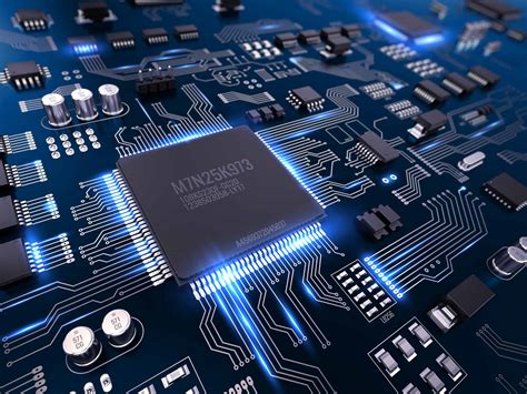
Complex Circuit Designs Made Possible by Additive Manufacturing
Additive PCB manufacturing is reshaping the landscape of electronics by enabling the creation of complex circuit designs that were previously unattainable with traditional methods. Thanks to the layer-by-layer approach, you can produce intricate geometries that optimize space and improve electrical performance. This method allows for the integration of multiple functionalities into a single board, streamlining design processes and reducing the number of components required. Many PCB manufacturing companies are now embracing this technology to meet the growing demand for more compact and efficient devices in the market. By utilizing advanced materials and innovative techniques, additive manufacturing facilitates tailored solutions that cater to specific application needs, ultimately enhancing product reliability. Moreover, you will find that as additive methods advance, they contribute significantly to lowering the overall PCB manufacturing cost, making high-quality circuits more accessible than ever before. This has given rise to new opportunities for various industries, allowing your PCB manufacturing business to stay competitive by adapting to these cutting-edge advancements in technology. As a result, you can expect a faster transition from initial concept to production while maintaining high standards of quality and performance.
Comparing Traditional and Additive PCB Manufacturing Methods
When evaluating pcb manufacturing methods, the differences between traditional and additive processes are significant. Traditionally, pcb manufacturing companies rely on subtractive techniques, where material is removed from a larger block to create the desired circuit patterns. This method can be effective but often presents challenges such as increased pcb manufacturing cost due to material waste and longer lead times. In contrast, additive PCB manufacturing builds the circuit layer by layer, which not only minimizes material waste but also allows for the production of highly complex designs that are difficult to achieve with traditional methods. You may find that with additive processes, the flexibility in design leads to quicker iterations and innovations in products, making your pcb manufacturing business more competitive in today’s fast-paced market. The efficiency of additive PCB manufacturing is evident as it enables rapid prototyping – thus shortening the time from concept to creation. As you weigh your options for pcb manufacturing, consider how embracing additive techniques can strategically benefit your operations and enhance your ability to meet evolving consumer demands successfully.
Future Trends in Additive PCB Technology
As you look ahead in the world of additive PCB manufacturing, several trends are destined to shape the landscape of pcb manufacturing companies and their operations. One notable trend is the continuous advancement in material science, which will enable manufacturers to utilize a broader range of materials, thus improving the performance and efficiency of printed circuit boards. This evolution not only reduces the pcb manufacturing cost but also opens up possibilities for complex circuit designs that were previously unimaginable. Additionally, you might observe a shift towards increased digitalization within the pcb manufacturing business, allowing for more streamlined processes and enhanced automation. Innovations such as real-time monitoring and AI-driven analytics will enable these companies to respond quickly to market demands while minimizing waste and production errors. As the industry embraces these technological developments, it will likely lead to an overall enhancement in product quality and customer satisfaction, positioning additive processes as a cornerstone of future electronics manufacturing. The ongoing evolution of additive technologies heralds not just changes but a fundamental reimagining of how you perceive and engage with electronic circuits in everyday life.
Case Studies: Success Stories in Additive PCB Implementation
Additive PCB manufacturing has begun to make waves in the electronics industry, as evidenced by various success stories that highlight its transformative potential. For instance, a leading PCB manufacturing company successfully utilized additive processes to reduce their PCB manufacturing cost significantly while improving production speed. By employing this innovative technique, they were able to create intricate designs that traditional methods struggled to facilitate, resulting in enhanced product functionalities.
In another case, a startup specializing in wearables partnered with an additive PCB manufacturing business to expedite their R&D process. The flexibility of additive methods allowed them to prototype rapidly at a fraction of the cost associated with conventional techniques. They could test and iterate on their designs seamlessly, reducing time-to-market and ensuring they stayed ahead of competitors. These case studies illustrate not only the efficiency improvements associated with additive manufacturing but also underscore its ability to foster creativity and innovation among electronics designers and engineers.
| Company | Industry | Challenge | Solution | Result |
|---|---|---|---|---|
| Tech Innovators Inc. | Consumer Electronics | High production costs with complex designs | Implemented Additive PCB Manufacturing | Reduced costs by 30%, faster prototyping |
| Smart Wearables Ltd. | Health Tech | Slow R&D cycles | Adopted 3D printing for PCBs | Time-to-market cut by 50% |
These examples serve as powerful testaments to how embracing additive PCB manufacturing can lead not only to significant operational efficiencies but also innovative breakthroughs that push the boundaries of what is possible in electronics design.
Conclusion
In reflecting on the transformative influence of additive PCB manufacturing, it’s clear that this innovative approach is not just a trend, but a vital shift for the pcb manufacturing landscape. The ability to create intricate designs without the limitations imposed by traditional methods empowers pcb manufacturing companies to explore novel concepts that were previously unattainable. You may appreciate the benefits of rapid prototyping, which allows for quicker iterations and significantly shorter time-to-market, a critical advantage in today’s fast-paced electronics sector. Furthermore, the implications on the pcb manufacturing cost are notably favorable; reduced material waste and streamlined production processes mean that businesses can not only save money but also reinvest in greater innovation and complexity in their circuit designs. This adaptability positions your pcb manufacturing business on a path of sustained growth and competitiveness, ensuring you remain at the forefront of technological advancements. As you contemplate future projects, embracing additive manufacturing could prove to be a game-changer in delivering high-quality, cutting-edge electronic solutions.
FAQs
What is additive PCB manufacturing?
Additive PCB manufacturing refers to a technology that builds printed circuit boards through a layer-by-layer process, allowing for greater design flexibility, particularly in complex structures. This method utilizes 3D printing technologies to create circuits instead of traditional subtractive manufacturing techniques.
What are the benefits of using additive PCB manufacturing?
The benefits include enhanced design capabilities, faster turnaround times for prototypes, and reduced PCB manufacturing costs. This process also enables customization without the limitations often found in traditional PCB manufacturing companies.
How does additive manufacturing speed up prototyping?
Additive PCB manufacturing enables you to quickly produce prototypes with intricate designs that would be time-consuming and costly through conventional methods. This rapid prototyping allows for expedited R&D processes, keeping your projects on schedule.
What is the impact of additive methodologies on the costs associated with PCB production?
Adopting additive techniques generally results in lower PCB manufacturing costs, particularly since less material waste occurs compared to traditional methods. The cost-effectiveness is an essential factor for many PCB manufacturing businesses, especially startups looking to minimize expenses while maximizing innovation.
Can additive PCB technology produce complex circuit designs?
Yes, one of the key advantages of this method is its ability to facilitate intricate circuit layouts that are difficult or impossible to achieve with traditional techniques. This offers significant opportunities for engineers and designers seeking advanced solutions.
For a deeper dive into how you can leverage these advancements in your projects, please click here: Additive PCB Manufacturing